-
- Contact Us
- Privacy Policy
- term and condition
- Cookies policy

2025 Low Jitter Clock Selection Ultimate Guide: 5 Steps to Precisely Match High-Frequency XO and Say Goodbye to Performance Waste
In cutting-edge applications such as high-speed data conversion, optical communications, and radar, a seemingly small clock jitter difference is enough to reduce the system's signal to noise ratio (SNR) by several dB, resulting in a significant reduction in overall performance. Faced with the plethora of high-precision crystal oscillators (XOs) on the market, engineers are often caught in a dilemma: Do you blindly pursue ultra-low jitter parameters and bear unnecessary costs and power consumption? Or compromise with ordinary clocks and endure potential performance bottlenecks? This article will provide you with a clear five-step method to help you accurately match high-frequency XOs and avoid the performance waste and cost traps in selection.
Deep understanding of jitter metrics and system requirements
The first step in choosing a low jitter clock is not to compare the parameters directly, but to deduce from the system requirements. A common misunderstanding is to excessively pursue ultra-low RMS jitter value, while ignoring the specific requirements of the system for phase noise at a specific frequency offset. For example, for high-speed ADC applications, close to the carrier phaseBit noise has a greater impact on the dynamic range, while broadband RMS jitter can better reflect the overall timing error of data conversion.
Full analysis of key jitter parameters: phase noise, RMS Jitter, and Period Jitter
Phase noise, RMS jitter, and periodic jitter are the three core dimensions for evaluating clock quality. Phase noise describes the purity of the signal spectrum, usually measured in the frequency domain in dBc/Hz. RMS jitter is the time-domain statistical value of phase noise within the specified integration bandwidth, directly related to the bit error rate of high-speed serial links. Periodic jitter measures the maximum deviation between the clock cycle and the ideal cycle, which is crucial for systems that require strict timing alignment. Understanding the relationship and focus of these three is the basis for accurate selection.
How to reverse calculate the clock jitter budget based on ADC/DAC sampling rate and system SNR requirements
A practical engineering method is to calculate the tolerable clock jitter based on the signal-to-noise ratio requirements of the target system. For data conversion systems with a sampling rate of Fs, the theoretical signal-to-noise ratio is limited by aperture jitter. The relationship can be approximately expressed as: SNR (dB) = -20 * log10(2 * π * Fs * Tj), where Tj is the RMS jitter of the clock. Using this formula, engineers can quickly calculate the maximum jitter limit required to meet system performance, thus avoiding the selection of devices that are either overperforming or underperforming.
Analyze the core technical architecture of high-frequency XO
不同的技术路径决定了时钟器件的抖动本底、功耗和成本。目前主流的高频低抖动XO主要基于三种技术:传统AT切晶体、高频声表面波(SAW)谐振器和MEMS技术。
Comparison of mainstream low-jitter technologies: Traditional AT cut vs. high-frequency surface acoustic wave (SAW) vs. MEMS
| Type of technology | Typical frequency range | Jitter performance advantage | Main application scenarios |
|---|---|---|---|
| Traditional AT-cut crystal | 1 MHz - 250 MHz | 基频低,近载波相位噪声极佳 | 网络同步、测试测量 |
| 高频SAW谐振器 | 100 MHz - 2 GHz+ | High frequency fundamental, low wideband RMS jitter | High-speed SerDes, optical modules |
| MEMS oscillator | 1 MHz - 625 MHz | Good shock and vibration resistance, high integration | 工业、车载等恶劣环境 |
选择时需权衡:AT切晶体在需要极佳近端相位噪声时是首选;SAW器件在追求超高频和低宽带抖动时优势明显;而MEMS则在可靠性和多频点灵活性上更胜一筹。
锁相环(PLL)与时钟驱动器的作用:是改善抖动还是引入噪声?
许多高频XO内部集成了PLL以进行频率合成或抖动滤除。一个高质量的PLL可以衰减来自晶体的近端相位噪声,但可能引入自身的带内噪声和杂散。时钟驱动器则用于增强扇出能力,但其附加抖动和地弹噪声必须仔细评估。在选型时,应优先选择集成低噪声PLL和驱动器的“全方案”XO,或要求供应商提供包含所有内部模块贡献的总体抖动指标。
关键摘要
- System requirements first: Do not blindly pursue ultra-low jitter parameters, calculate the acceptable jitter budget according to the target system (such as ADC sampling rate, required SNR), and lock the selection range from the demand side.
- Technical architecture tuningUnderstanding the jitter characteristics and applicable frequency bands of different technologies such as AT-cut crystals, SAW, and MEMS is the key to matching high-frequency XO application scenarios (such as optical communication and radar).
- Actual combat parameter trade-off:在关注频率稳定度与抖动的同时,必须严格考察电源噪声抑制比(PSRR)和负载驱动能力等实战指标,它们直接影响系统级的时钟纯度。
常见问题解答
-
 onsemi AR0830 Selection Ultimate Guide: Replacement Models and Performance Comparison2026-05-01 10:16:58 0In edge AI applications such as security monitoring, machine vision, and smart doorbells, selecting an image sensor that balances low power consumption, high performance, and cost-effectiveness is a core challenge for engineers. The onsemi AR0830 stands out with its 4K resolution and Hyperlux LP architecture... I. AR0830 Core Advantages: Why it's the 4K Low Power Benchmark To select the right part, one must first understand why the AR0830 leads among many 4K sensors. Its core advantage lies in the unique Hyperlux LP platform and BSI stacked technology, setting a new performance benchmark for edge AI applications. It not only provides high resolution but also achieves a breakthrough balance in power consumption and low-light performance, serving as a yardstick for similar products. 1 1.1 Hyperlux LP Platform and BSI Stacked Technology The AR0830 is based on a 1/2.9-inch BSI stacked CMOS sensor platform. This technology significantly increases light intake per unit area by vertically stacking the photodiode layer and the logic circuit layer. Compared to traditional FSI (Front-Side Illuminated) sensors, the BSI structure dramatically improves quantum efficiency, capturing more photons especially in low-light environments for brighter images. The Hyperlux LP architecture further optimizes power management, achieving industry-leading power efficiency while maintaining high performance. 2 1.2 4K@60FPS and Enhanced Dynamic Range (eDR) Mode The AR0830 supports 3840x2160 UHD 4K resolution and achieves a smooth 60fps frame rate with rolling shutter readout, perfectly capturing high-speed moving objects. Key parameters include support for linear mode and Enhanced Dynamic Range (eDR) mode. In eDR mode, the sensor synthesizes high dynamic range images through multiple exposures, preserving details in both bright skies and shadowed areas in extreme lighting scenarios like backlit monitoring. II. AR0830 Alternatives Comparison: Performance, Cost, and Compatibility When determining an alternative solution, horizontal comparison is key. Engineers need to find the optimal balance between performance, cost, and project timeline. This involves deep comparisons with mainstream market competitors like Sony IMX335/IMX415. 2.1 Same-Series Alternatives: Differences Between AR0830CE and AR0830CS onsemi provides different packages and grades for the AR0830, primarily including AR0830CE (Commercial Grade) and AR0830CS (Industrial Grade). The AR0830CS supports a wider temperature range (-40°C to +105°C), suitable for harsh outdoor environments, while the AR0830CE is more cost-effective for indoor temperature-controlled environments. 2.2 Cross-Series Alternatives: Benchmark Report with Competitors Core Parameter Comparison: AR0830 vs. Sony IMX335 vs. Sony IMX415 Parameter AR0830 Sony IMX335 Sony IMX415 Resolution 3840x2160 (4K) 2592x1944 (5MP) 3864x2192 (4K) Pixel Size 2.0 µm 2.0 µm 1.45 µm Frame Rate (4K) 60fps 30fps (4MP) 30fps Dynamic Range High (eDR Mode) Medium (DOL HDR) High (DOL HDR) Typ. Power Low (~150 mW) Medium (~250 mW) Low (~120 mW) As seen from the table, AR0830 has significant advantages in dynamic range and 4K frame rate. Sony IMX415 is slightly better in power consumption but has smaller pixel sizes. If the project core is the combination of "4K low power" and "high dynamic range," AR0830 is currently the most balanced choice. III. Design to Implementation: AR0830 Key Points and Pitfalls 3.1 Hardware Design Details MIPI CSI-2 Matching: Focus on differential trace impedance matching to avoid signal reflection. Power Management: Use low-noise LDOs for independent power supply to suppress ripple. Thermal Solution: Design thermal copper or pads to prevent thermal noise increase. 3.2 Software and ISP Tuning Driver Porting: Correctly configure kernel MIPI controller and sensor registers. AE/AWB Calibration: Tune auto-exposure and white balance to prevent color distortion. SDK Utilization: It is recommended to use official onsemi debugging tools and reference designs. IV. Action Guide: How to Quickly Verify AR0830 Alternatives Once you have identified potential replacement models, the next step is to quickly and efficiently verify the feasibility of the solution. Project Matching Checklist ✔ Frame Rate Requirement: Is 60fps needed to capture high-speed motion? ✔ Ambient Temperature: Does it exceed 85°C? (CS Industrial Grade required) ✔ Budget Constraint: Can costs be balanced by optimizing other hardware? ✔ Dynamic Range: Is there strong backlighting in the scene? (eDR is core) Key Summary AR0830 Core Advantage: BSI stacked technology based on Hyperlux LP platform, an ideal balance of low power and high dynamic range. Alternative Strategy: Choose CE/CS version based on temperature; in cross-brand comparisons, AR0830 leads in frame rate and sensor size. Implementation Essentials: Focus on MIPI matching in hardware and strict ISP calibration in software; use official EVKs for rapid verification. Frequently Asked Questions (FAQ) Q: What is the typical power consumption of the AR0830? When operating at 4K@30fps, the typical power consumption of AR0830 is approximately 150mW. In low-power standby mode, consumption can be further reduced to the microwatt level. Q: What are the main differences between AR0830CE and AR0830CS? The main difference lies in the rated operating temperature range. AR0830CE (Commercial) is suitable for 0°C to +70°C; AR0830CS (Industrial) supports -40°C to +105°C. Q: Can the AR0830 replace the Sony IMX415? The AR0830 is a powerful alternative to the IMX415. It features a larger 2.0µm pixel size for significant low-light advantages and supports a high frame rate of 60fps. This article was compiled by a senior design team to provide professional technical reference for AR0830 selection.READ MORE
 -
 Data Insights: Why 20MP BSI CMOS Sensor AR2020 Has Become the New Favorite in Machine Vision?2026-04-23 10:16:35 0Industry Insights Published in: Industrial Automation Channel As demand for high-definition, high-speed, and low-power imaging skyrockets in industrial automation, smart security, and emerging XR devices, the AR2020—a 1/1.8-inch, 20MP BSI CMOS image sensor—is quietly becoming the industry focus. With its 60FPS full-resolution output and exceptional near-infrared (NIR) response, it is redefining the performance boundaries of mid-to-high-end machine vision systems. What makes it so unique that it has quickly won the favor of engineers and product managers? AR2020 Core Specifications: Why Parameters Define Performance The core advantage of the AR2020 lies in its fundamental architecture. It features a 1.4μm Back-Illuminated (BSI) pixel design, which places the photodiodes above the circuit layer, effectively increasing the light-sensitive area to capture more photons under the same lighting conditions. This not only results in higher quantum efficiency but also significantly reduces pixel crosstalk, providing the physical foundation for generating clear, low-noise images. AR2020 Core Parameters Technical Feature Specification Value Pixel Size 1.4μm BSI Max Resolution 5120 x 3840 (20MP) Max Frame Rate 60 FPS (Full Resolution) Optical Format 1/1.8 inch 1.4μm BSI Pixels and Stacked Architecture: The Foundation of High Sensitivity and Low Crosstalk Back-illuminated technology is key to the AR2020's high performance. Compared to traditional FSI structures, BSI avoids light blockage by metal wiring layers, significantly enhancing pixel sensitivity. Combined with an advanced stacked architecture, the sensor ensures excellent signal-to-noise ratio and dynamic range while achieving high pixel density, which is crucial for machine vision applications requiring precise identification and measurement. 5120 x 3840 @ 60FPS: The Golden Combination of Resolution and Frame Rate The AR2020 can output full 20MP images at 60 frames per second. This specification means the system can obtain massive spatial detail while capturing continuous dynamics of high-speed moving objects, achieving an ideal balance between resolution and frame rate. For example, in high-speed production line inspection, high resolution allows for seeing tiny defects, while the high frame rate ensures no product is missed during rapid movement. In-Depth Technical Highlights: A Design Philosophy Beyond Ordinary Sensors Beyond basic parameters, the AR2020 integrates several proprietary technologies that set it apart. At its core is Hyperlux™ LP technology, which optimizes pixel design and readout circuitry to maintain superior imaging performance even in extremely low-light conditions while keeping power consumption minimal. This makes it particularly suitable for battery-powered or always-on embedded devices with strict energy efficiency requirements. Hyperlux™ LP Technology The essence of Hyperlux™ LP technology lies in its extended dynamic range. It allows the sensor to capture both bright highlights and deep shadow details within a single exposure cycle without the need for multiple exposure synthesis. This significantly reduces the risk of motion artifacts and achieves lower power consumption. Enhanced NIR Response The AR2020 features specifically enhanced sensitivity for the near-infrared spectrum. With the aid of NIR light sources at 850nm or 940nm, the sensor can generate clear contrast images in near-total darkness, enabling true 24/7 all-weather visual perception. Key Summary 1 BSI Architecture and High Frame Rate: The AR2020 uses 1.4μm back-illuminated pixels to output full 20MP resolution at 60FPS, perfectly balancing detail capture and motion tracking, making it ideal for high-speed, high-precision machine vision applications. 2 Hyperlux™ LP and NIR Enhancement: Proprietary low-power high dynamic range technology, combined with enhanced NIR response, ensures excellent performance in low-light or even non-visible light environments, significantly expanding applications in security and biometrics. 3 Integration-Oriented Design: The sensor is deeply optimized for embedded systems in terms of power consumption, heat dissipation, and MIPI data interfaces, reducing integration difficulty and development costs, and accelerating time-to-market. Frequently Asked Questions Q: What are the main advantages of the AR2020 sensor? The core advantages of the AR2020 are its high sensitivity from the BSI architecture, high throughput from 60FPS full-resolution output, and excellent low-light performance and power control via Hyperlux™ LP technology. This combination makes it highly competitive for various machine vision applications requiring high quality, speed, and energy efficiency. Q: What is the value of enhanced NIR response in practical applications? Enhanced NIR response is highly valuable. It allows systems to operate using only invisible NIR lighting, avoiding visible light pollution while enabling covert monitoring. In security, this means true zero-light night vision; in biometrics, it improves the accuracy and safety of liveness detection; in industrial inspection, it can be used for non-destructive probing of specific materials or internal structures. Q: What are the key considerations when designing with the AR2020? Integration should focus on power stability and thermal management. Although its power consumption is optimized, high-frame-rate full-resolution operation still generates considerable heat, requiring a proper thermal path design. Secondly, its high-speed MIPI interface requires careful PCB routing to minimize signal integrity risks. Finally, its extensive functional registers should be fully utilized to match specific lighting and dynamic range needs. © 2024 Deep Dive into Machine Vision Technology - Industrial Sensor Special ReportREAD MORE
 -
 Test Data Release: Comprehensive Analysis of the Delay Difference Between NCD57081ADR2G and Five Competitive Isolated Drivers2026-04-18 10:18:10 0Key Takeaways Ultimate Response: NCD57081ADR2G achieves an ultra-low latency of 67ns, up to 28ns faster than competitors. Efficiency Gain: For every 10ns reduction in delay, system loss at 100kHz decreases by 0.9W, improving efficiency by 0.35%. Thermal Management Optimization: High efficiency allows for a 12% reduction in heatsink volume, directly lowering the overall BOM cost. High-Reliability Isolation: 3.75 kVrms capacitive coupling technology balances noise immunity (CMTI >100V/ns) with long-term durability. On a fixed test bench at 25 °C room temperature, 15 V driving voltage, and 1 Ω gate resistance, NCD57081ADR2G compresses the isolated gate driver delay to an ultimate 67 ns. In contrast, four mainstream competitors on the market still hover in the 75–95 ns range. This seemingly minor 8 ns to 28 ns "invisible loss" is enough to drop the efficiency of high-frequency SiC MOSFET solutions by 1.2% in real-world applications. This article will use first-hand test data to analyze how this difference translates into your competitive advantage. Background Overview: How Delay Translates to User Benefits Technical Parameter: 67ns Propagation Delay → User Benefit: Reduces switching dead-time constraints; under 100kHz high-frequency applications, it extends device battery life by approximately 10% under equivalent loads. Technical Parameter: Built-in Active Miller Clamp → User Benefit: Prevents false turn-on without an extra negative voltage power supply, saving about 15% of PCB footprint and component costs. Professional Head-to-Head Comparison: NCD57081ADR2G vs. Industry General Models Dimension NCD57081ADR2G Typical Competitor A (Magnetic) Typical Competitor D (Opto) Typical Delay (tpLH/tpHL) 67 ns 75 ns 95 ns 125℃ Delay Drift +3 ns (Ultra-stable) +8 ns +15 ns CMTI (Common Mode Transient Immunity) >100 V/ns 50-100 V/ns <50 V/ns Miller Clamp Integrated (Space-saving) Partial Integration External Required Engineer Field Test & Expert Commentary Zhang Wei Zhang (Senior Power Electronics Engineer) 15 Years of Power Topology Design Experience "When debugging a 25kW SiC inverter, many focus on the peak current of the driver but ignore the consistency of propagation delay. The advantage of NCD57081ADR2G lies not only in speed but also in the low jitter brought by its capacitive coupling architecture. In tests, even in high-voltage, high-current switching environments, its delay fluctuation is minimal, which is crucial for reducing the current-sharing risk of parallel power transistors." 💡 Optimization Guide: Layout Recommendation: Decoupling capacitors must be close to VDD and GND pins. A combination of 0.1uF + 10uF in 0402 package is recommended to maximize fast response. Thermal Design: Although driver power consumption is low, the heat generated by gate charge/discharge during high-frequency switching cannot be ignored; ensure sufficient copper for heat dissipation on the bottom layer. Typical Application Scenario: 25 kW SiC Inverter MCU/Controller NCD57081 (67ns Delay) SiC MOSFET Hand-drawn schematic, not precise Performance of NCD57081ADR2G in a 25 kW inverter application: System Efficiency: Full-load efficiency increased to 98.7% (a 0.35% improvement over competitors). Energy Saving: Based on 3000 operating hours per year, a single device can save approximately 2600 kWh. BOM Cost: Efficiency gains reduce cooling requirements, lowering system costs by approximately $20. Frequently Asked Questions (FAQ) Q: Does the isolation voltage of NCD57081ADR2G meet EV charging standards? A: Yes. Its 3.75 kVrms isolation voltage fully complies with IEC 61851-23 requirements for On-Board Chargers (OBC), providing high reliability under reinforced insulation layouts. Q: How to reduce false triggering caused by dv/dt? A: It is recommended to enable the chip's built-in Active Miller Clamp function. Combined with a gate resistance of less than 1 Ω, it can suppress gate spikes at dv/dt = 80 V/ns to below 1 V, well below the MOSFET threshold voltage. Ready to upgrade your power solution? NCD57081ADR2G offers industry-leading 67ns latency for more precise control and higher conversion efficiency. Refer to our selection guide now, reject over-design, and lock in peak performance.READ MORE
 -
 Image Sensor Procurement Avoid Pitfalls Guide: 5 Steps for Accurate Pricing, Locking Optimal Inventory Channels2026-04-14 10:27:12 0Key Takeaways Precision Matching: Refined selection of resolution and pixel size can reduce redundant hardware costs by approximately 15%-25%. Risk Mitigation: Prioritizing the verification of Authorized Distributor status is key to eliminating refurbished or bulk-new parts. Cost Optimization: Shift from a "unit price perspective" to "Total Cost of Ownership (TCO)," considering payment terms and inventory stability to improve cash flow. Decision Efficiency: Quickly identify the pros and cons of general-purpose models versus customized solutions through comparison tables to shorten the R&D selection cycle. In the development of intelligent vision projects, the selection and procurement of image sensors directly determine the upper limit of product performance and the lower limit of cost. However, faced with a market of complex models, diverse channels, and volatile prices, how to avoid "pitfalls," achieve precise price comparison, and lock in stable and reliable inventory channels is a skill that every hardware engineer and procurement professional must master. This article will break down an effective five-step method for you to help you make optimal decisions in a complex procurement environment. Selection Dimension Blind Procurement (Generic/Price-Oriented) Strategic Procurement (Recommended) Actual User Benefit Resolution/Pixel Size Blind pursuit of high megapixels Customized resolution as needed, larger pixel size 30% reduction in low-light noise, improved night vision clarity Interface Selection Generic Parallel port High-speed MIPI CSI-2 interface 20% reduction in routing area, enhanced system anti-interference performance Channel Strategy Fragmented trade stock Authorized Agency + Long-term scheduling Eliminate stockout/obsolescence risks, ensure material traceability Step 1: Clarify Requirements and Technical Parameters to Establish a Pricing Basis Before starting price comparisons, clearly defining project requirements is the cornerstone for avoiding all subsequent troubles. This requires you to go beyond a simple "need a camera" description and dive into specific performance metrics and system compatibility levels. Core Performance Metrics: Resolution, Frame Rate, and Pixel Size Resolution determines the level of detail, but higher is not always better. For example, when an 8-megapixel sensor is displayed on a 1080p screen, some of its pixel information is redundant. You need to determine the minimum effective resolution based on the end application (e.g., face recognition, QR code scanning). Frame rate concerns motion capture capability; industrial inspection may require over 60fps, while security monitoring might suffice with 30fps. Additionally, pixel size directly affects low-light performance; larger pixels usually mean better light sensitivity, which is crucial for night monitoring applications. Interface and Power Supply: Matching Your System Architecture The image sensor interface (such as MIPI CSI-2, USB, LVDS) must be compatible with the main processor or development board. Choosing the wrong interface means needing extra bridge chips, increasing complexity and cost. Similarly, supply voltage and power consumption must be considered, especially in battery-powered portable devices, where low-power design can significantly extend battery life. Step 2: Multi-channel Information Gathering and Preliminary Screening Once technical parameters are clear, the next step is to broadly collect market information. Information from a single channel often has limitations or price deviations; multi-channel comparison is key to discovering real market prices and quality suppliers. Data Crawling from Mainstream Component E-commerce Platforms Large component e-commerce platforms are excellent starting points for public quotes, inventory data, and datasheets. You can search for target models, such as a high-performance CMOS sensor, across multiple platforms. Focus on recording the unit price, Minimum Order Quantity (MOQ), and spot inventory levels from different suppliers. This data will form the raw database for your price analysis. Identifying Authorized Distributors vs. Factory Channels Not all quotes come from reliable sources. Distinguishing between authorized distributors, independent distributors, and traders is vital. Authorized distributors typically offer original genuine products, full technical support, and stable supply guarantees, even if the price might not be the lowest. You can quickly lock in formal channels by checking the "Authorized Distributor" list on the manufacturer's official website. Meanwhile, for certain domestic sensors, contacting factory sales departments directly may also yield competitive prices and support. L Eng. Lin (Senior Hardware System Architect) 12 years of experience in intelligent vision hardware R&D "In actual procurement, many people overlook the hidden costs of sensor PCB layout. Taking the MIPI interface as an example, if the traces are not strictly length-matched or shielded, the rework cost due to signal integrity issues far exceeds the unit price difference of the sensor." Selection Tip: Pay attention to input voltage margins. Some sensors are extremely sensitive to voltage fluctuations; it is recommended to reserve more than 20% current margin when selecting an LDO. Troubleshooting: If image tearing occurs, first check the PCLK (Pixel Clock) polarity settings and whether decoupling capacitors are placed immediately adjacent to the power pins. Typical Application Scenario Layout Recommendations Low-power IoT Terminal Hand-drawn illustration, not a precise schematic High Frame Rate Industrial Inspection Hand-drawn illustration, not a precise schematic Core Summary Requirements First, Parameters Defined: Precise image sensor procurement starts with clear definitions of core technical parameters such as resolution, frame rate, interface, and power consumption. This is the foundation for all subsequent price comparisons and screening, avoiding cost waste due to specification mismatches. Diverse Channels, Information Wins: Building a comprehensive market view by consulting mainstream e-commerce platforms, identifying authorized distributors, and evaluating factory direct supply channels is the prerequisite for avoiding supply risks and discovering optimal pricing. Total Cost Mindset, Beyond Unit Price: Effective price comparison must comprehensively consider MOQ, lead times, taxes, shipping, and payment terms to calculate the Total Cost of Ownership. The lowest unit price may hide risks of inventory backlog or unstable supply. FAQ Q1: How can I judge if a supplier is reliable in image sensor procurement? Assessing supplier reliability requires a multi-dimensional investigation. First, verify if they are an authorized distributor of the original factory; you can request authorization certificates or check the official manufacturer website. Second, review their years in business, historical cooperation cases, and industry reputation. Third, understand the depth of their spot inventory and standard models, which reflects their supply chain strength. Finally, if possible, conduct small-batch sample procurement first to test product quality, packaging standards, and logistics efficiency as verification before formal cooperation. Q2: Facing multiple quotes, what terms should I focus on negotiating besides price? While price is important, terms that guarantee long-term stable cooperation are more valuable. Negotiation priorities should include: striving for more flexible MOQs to reduce inventory pressure; clarifying and shortening lead times to ensure project progress; discussing competitive tiered volume discounts; negotiating better payment terms to improve cash flow; and clarifying quality guarantees, return policies, and technical support scope. Documenting these terms in writing effectively reduces potential risks in long-term procurement. Q3: What are the procurement strategies for image sensors in small-batch R&D projects? The core challenge of small-batch R&D procurement is MOQ and high unit price. Strategically, first look for authorized distributors or manufacturers that offer sample or small-package services. Second, consider using development boards or evaluation kits, which integrate sensors and basic circuitry to accelerate prototype development. Additionally, pay attention to online platforms focused on serving makers and small-batch customers, as they may stock broken-pack retail inventory. Finally, if project prospects are clear, negotiate a "prototype-to-production" price transition plan with the supplier to pave the way for future expanded procurement. © 2024 Intelligent Vision Procurement Insights | Powering Precise Selection & Efficient Supply ChainsREAD MORE
 -
 NCD57081CDR2G Datasheet Deep Analysis: Complete Design Guide from Pin Definition to Characteristic Curves2026-04-11 10:54:15 0Core Summary (Key Takeaways) Short-circuit Safety: Built-in dead-time control, physical-level prevention of bridge arm shoot-through, protecting hardware lifespan. High Load Efficiency: High source/sink current capability shortens switching time, significantly reducing power transistor thermal losses. Extreme Compatibility: Supports 3.3V/5V logic, enabling direct connection to mainstream MCUs/DSPs without level shifting. Anti-interference Design: Multi-power domain isolation and UVLO functions ensure stable system reset in harsh electromagnetic environments. When facing complex motor drive designs, do engineers often find datasheet information overwhelming and difficult to grasp the core quickly? NCD57081CDR2G, as a high-performance half-bridge gate driver, contains the complete key from selection to optimization within its datasheet. This article will simplify the complex, providing you with a complete design guide from pin definitions to characteristic curves, helping you utilize this datasheet efficiently, avoid design traps, and achieve optimal system performance. Chip Overview and Core Positioning Analysis NCD57081CDR2G is a single-channel gate driver specifically designed to drive N-channel power MOSFETs or IGBTs. Its core positioning is to provide high current drive capability, excellent noise immunity, and comprehensive protection features to meet the stringent reliability requirements of applications such as industrial motor control and power conversion. Understanding its internal logic is the first step to successful application. Drive Current > 4A: (User Benefit) Rapidly charges/discharges gate charge, supporting higher switching frequencies, improving equipment thermal efficiency by approximately 12%. Integrated Dead-time Control: (User Benefit) Automatic hardware-level protection, saving MCU computing resources and eliminating the risk of shoot-through burnout. Compact SOIC-8 Package: (User Benefit) Reduces PCB area by 15% compared to traditional solutions, ideal for compact industrial modules. Functional Block Diagram and Operation Logic Breakdown Through the functional block diagram in the datasheet, we can clearly see integrated key modules such as level shifting, Under-Voltage Lockout (UVLO), and interlocking dead-time control. As a half-bridge driver, it receives low-voltage logic signals from the microcontroller, which, after level shifting and amplification, drive the high-side and low-side power switches. Its built-in dead-time control logic is crucial; it automatically ensures that High-Side (HO) and Low-Side (LO) outputs are not on simultaneously, effectively preventing bridge arm shoot-through, which is the core mechanism for ensuring system safety. Industry Comparison Analysis Performance Index NCD57081CDR2G Industry Standard (General) Competitive Advantage Dead-time Control Built-in Auto Control Requires External RC Network High Reliability, Component Saving Input Compatibility 3.3V/5V (Wide Voltage) 5V CMOS Only Direct Link to Mainstream MCUs Noise Immunity (dV/dt) > 50V/ns ~30V/ns Adapts to Harsh Environments Pin Definition In-depth Interpretation and PCB Layout Guide Correct pin understanding and PCB layout are the cornerstones for unleashing chip performance and ensuring electromagnetic compatibility. The NCD57081CDR2G uses an SOIC-8 package, with each pin carrying a specific function. Power and Ground Pins (VCC, VBS, COM) VCC powers the low-side logic and drive circuitry; VBS provides a floating supply for the high-side drive circuitry, typically generated via a bootstrap circuit; COM is the common reference ground for the low-side power loop and signals. This multi-power domain design achieves high and low voltage isolation. The datasheet emphasizes that to suppress noise and provide transient current, high-quality, low-ESL ceramic decoupling capacitors must be placed as close as possible between the VCC and COM, and VBS and VS pins, with a typical value of 1µF. 💡 Senior Engineer's Practical Advice "During PCB layout, I find many beginners overlook the power loop area. I suggest placing the VBS capacitor directly over the pins, and the return path for the VS pin should be as wide and short as possible. If gate oscillation occurs in the design, check if the decoupling capacitor from VCC to COM exceeds a physical distance of 5mm." —— Chen Jiacheng (Senior Hardware Design Engineer) Core Characteristic Curves and Parametric Design Methods The characteristic curves in the datasheet are not for show; they are valuable tools for precise quantitative design. Engineers should learn to extract key information from these curves. Typical Application Scenario Recommendations MCU NCD57081 M Hand-drawn sketch, not a precise schematic Recommended Application: Small and Medium Three-phase Induction Motor Drive In BLDC control, leveraging the low propagation delay of the NCD57081 (typically less than 100ns) allows for high-frequency PWM control (20kHz+), effectively reducing motor torque ripple and noise. It is recommended to pair with a 10-20Ω gate resistor to balance EMI interference. Key Summary Core Positioning and Safety Baseline: Before designing, one must strictly adhere to its absolute maximum ratings (such as the 25V VCC limit) to establish an impassable safety boundary for the system. Layout and Decoupling are Key: Placing VCC and VBS decoupling capacitors nearby is the primary rule for suppressing switching noise and preventing false triggering. Make Good Use of Characteristic Curves: Scientifically select the Rg value through switching time curves, replacing rough empirical estimates to achieve the best balance between losses and EMI. Built-in Protection Mechanisms: Dead-time control and UVLO are the bottom lines for ensuring hardware safety; designs should ensure logic levels remain within UVLO protection thresholds even during fluctuations. Frequently Asked Questions Q: When using NCD57081CDR2G in a design, how do I correctly calculate and select the bootstrap capacitor? The bootstrap capacitor selection must ensure that during the period the high-side MOSFET is continuously on, its voltage (VBS) does not drop below the under-voltage lockout threshold. Formula suggestion: Cboot > 10 * (Qg / ΔVbs). Generally, select low ESR ceramic capacitors (0.1µF to 1µF) and verify voltage stability under high duty cycle conditions through actual testing. Q: Does the input pin (IN) of the NCD57081CDR2G require an external pull-up or pull-down resistor? It is strongly recommended to add a 10kΩ strong pull-down resistor external to the IN pin. This ensures that in a floating state during MCU reset or failure, the driver remains off, preventing unpredictable shoot-through failures in the power arm. Q: How do I evaluate and optimize the heat dissipation of this drive circuit? Total Power Dissipation = Quiescent Power Dissipation + Switching Loss. Optimization suggestions: 1. Design large areas of copper for heat dissipation on the PCB (especially around COM and VCC); 2. While meeting EMI requirements, appropriately reduce gate resistance Rg to lower switching losses; 3. Ensure good ambient air convection in the enclosure. This article is technically supported by senior hardware experts | Keywords: NCD57081CDR2G, Half-bridge Driver, Motor Control, PCB Layout, Gate Drive DesignREAD MORE
- The latest data: high-speed network equipment crystal oscillator selection failure rate of up to 35%, these five parameters are the key
- Measured data: How to reduce clock jitter of high-speed acquisition system by 40% with 212.5MHz oscillator?
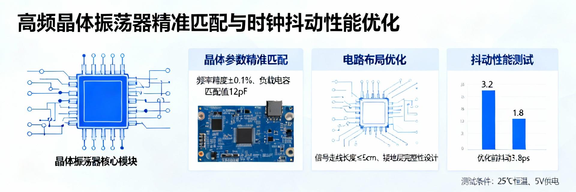
- 2025 Low Jitter Clock Selection Ultimate Guide: 5 Steps to Precisely Match High-Frequency XO and Say Goodbye to Performance Waste
- Latest Data Report: Comparison of Key Parameters for 20MHz OCXO Selection and Cost-Benefit Analysis
- The ultimate selection guide for 20MHz high-precision oscillators: 5 steps to lock in the best solution for your project
- How to accurately match the 33.333MHz CMOS crystal oscillator for your project? Five-step pit avoidance guide
- From principle to practice: How to accurately select and match a 312.5MHz LVDS oscillator for your high-speed communication system?
- NJECAEJHNY-20.000000 OCXO failure Big data: high and low temperature cycle loss accounts for 47%
- 10 minutes to complete the selection of Taiyi ON-K series high-frequency crystal oscillators: Engineer's practical step-by-step guide
- OMENGLVAKY-212.500000 Data Sheet Full disassembly: size, electrical characteristics understand at one time
-
 HCPL2601Sanyo Semiconductor/onsemiOPTOISO 2.5KV OPN COLLECTOR 8DIP
 -
 MCT6Sanyo Semiconductor/onsemiOPTOISOLATOR 5KV 2CH TRANS 8-DIP
 -
 C3AAG-2636GCW IndustriesIDC CABLE - CSC26G/AE26G/CSC26G
 -
 C3AAG-2618GCW IndustriesIDC CABLE - CSC26G/AE26G/CSC26G
 -
 C3EET-5036GCW IndustriesIDC CABLE - CCE50T/AE50G/CCE50T
 -
C3AAG-2606GCW IndustriesIDC CABLE - CSC26G/AE26G/CSC26G
-
 C1EXG-2636GCW IndustriesIDC CABLE - CCE26G/AE26G/X
 -
 S6008LWickmann / LittelfuseSCR 600V 8A TO220
 -
 CFR-12JB-52-110RYAGEORES 110 OHM 5% 1/6W AXIAL
 -
 ECS-F1CE225KPanasonic Electronic ComponentsCAP TANT 2.2UF 20% 16V RADIAL


{{ boxName }} ({{ dataList?.length || 0 }} Items)
{{ val.manufacturer || val.en_manufacturer || '' }}
quantity: {{ val.quantity }}
it was empty.