


帮助您节省成本和时间。

为您的货物提供可靠的包装。

快速可靠的交付以节省时间。

优质的售后服务。
新品上市
更多 +


热卖零件


博客
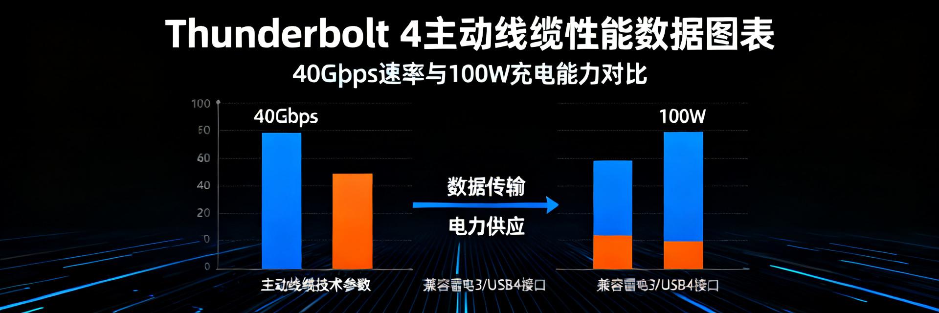
2米主动式Thunderbolt 4线缆深度评测:40Gbps与100W充电实测数据
当你的桌面需要一根2米长的Thunderbolt 4线缆时,为什么选“主动式”远比选“被动式”更重要?在40Gbps的极限带宽下,信号每多走一米,衰减的风险就成倍增加。市面上2米长的主动式Thunderbolt 4线缆,真的能兼顾40Gbps满速传输与100W稳定供电吗?本篇评测,我们将通过实打实的测试数据,撕开营销话术,深挖这款线缆的真实性能表现,看看它是否值得为你的生产力买单。 2米“主动式”…
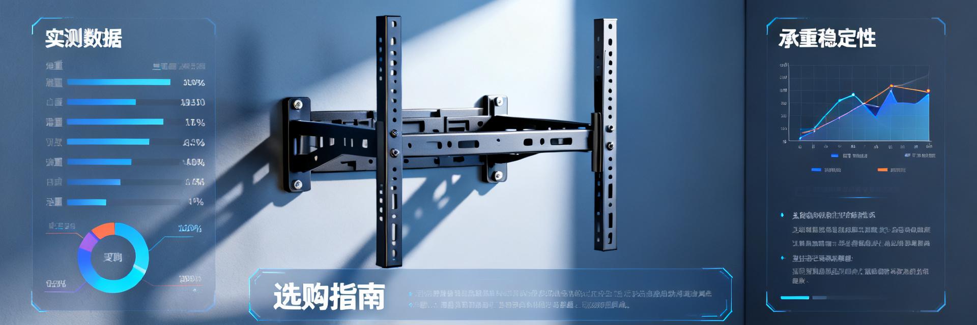
2025年壁挂主机架选购指南:3组实测数据告诉你哪款最稳
2025年,中国桌面收纳市场规模突破80亿元,其中壁挂主机架品类同比增长高达45%。在电商平台搜索“壁挂主机架”,结果超过10万条,价格从29元到299元不等。面对琳琅满目的选择,你真的知道哪款能稳稳托住你的主机吗? 我们以“承重稳定性”、“安装适配性”、“空间利用率”三大核心指标,对淘宝、京东上销量TOP20的壁挂主机架进行了3组深度实测。数据不会说谎,这份2025年实测选购指南,帮你一步到位选…