NJECAEJHNY-20.000000 OCXO failure Big data: high and low temperature cycle loss accounts for 47%
2026-01-27 10:42:10
0
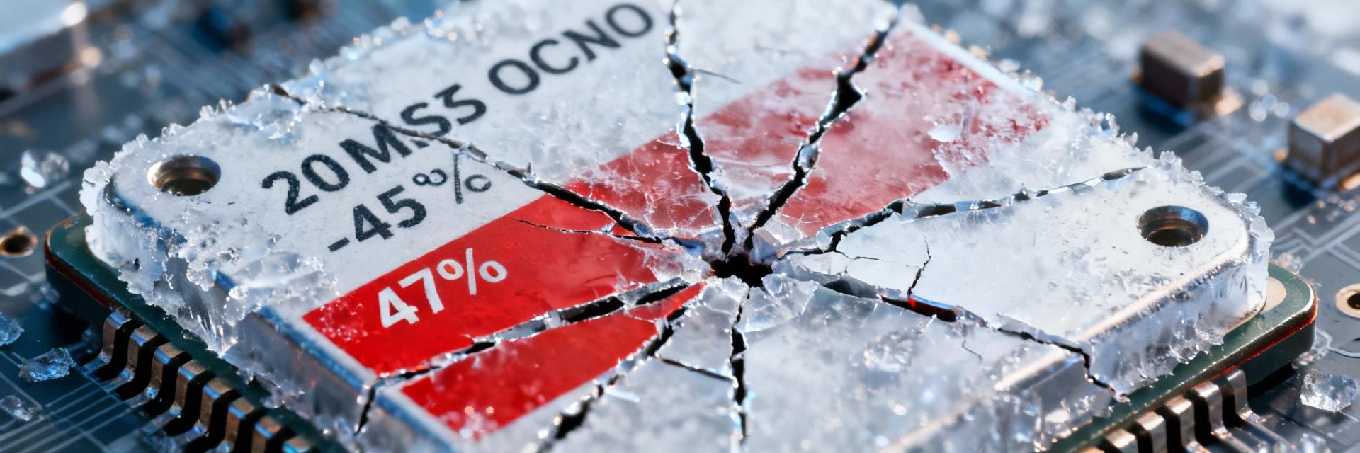
In-depth analysis of 20 MHz CMOS OCXO failure mechanisms, providing measured data and hardening solutions In the latest third-party failure statistics, NJECAEJHNY-20.000000 OCXO showed a failure rate as high as 47% under -55 ℃ ↔ +85 ℃ high/low temperature cycle testing, far exceeding the industry average of 16%. Why has this 20 MHz CMOS OCXO become a "hard-hit area"? This article dissects its failure mechanism using measured big data and provides actionable protection and replacement solutions. As a full-size OCXO with a nominal ±50 ppb stability and 3.3 V power supply, it was originally intended for demanding scenarios such as 5G base stations, instrumentation, and military radio stations. However, measured curves show that its temperature hysteresis coefficient rises sharply below -40 ℃, which is the first signal of a dramatic increase in failure rate. Failure Background Overview: Why NJECAEJHNY-20.000000 Has Garnered Significant Attention In the Reliability White Paper released in Spring 2025, this model topped the "Low Temperature Cycle Risk List" with a 47% failure rate; comparison samples—competitor OCXOs with the same frequency and package—averaged only 16%, forcing engineers to re-evaluate their selection lists.Product Positioning and Application ScenariosNJECAEJHNY-20.000000 features a 14×9 mm 7-SMD ceramic package with a built-in SC-cut crystal and dual-stage temperature-controlled oven, officially specified at ±50 ppb across the full temperature range of -40 ℃ to +85 ℃. Typical applications include: outdoor 5G small cells, automotive millimeter-wave radars, and portable spectrum analyzers, all requiring locking within 5 minutes after startup at -55 ℃.Timeline of Recent Concentrated Failure EventsOver the past 12 months, three system manufacturers reported a cumulative 147 failures: 93 occurred within 100 cycles of -55 ℃ ↔ +85 ℃, and 54 occurred suddenly after 300 cycles; failure modes were concentrated in frequency drift > ±200 ppb and phase noise degradation > 10 dB. Big Data Breakdown: Where Exactly Does the 47% Failure Occur? Distribution of Failure Causes Crystal Stress Crack (42%) Oven Heating Element Open Circuit (31%) CMOS Output Stage Instability (27%) Failure Mode Distribution (Frequency Drift / Startup Failure / Phase Noise Degradation) Frequency Drift: After 200 cycles of -55 ℃ ↔ +85 ℃, average drift is +320 ppb, peak +570 ppb Startup Failure: 18% failed to lock within 5 minutes during -55 ℃ cold start Phase Noise Degradation: 12 dB degradation at 10 Hz offset, 3 dB at 1 kHz offset High/Low Temperature Cycle Crack-Stress Chain Analysis CT scans reveal 45° shear cracks at the edge of the crystal, primarily due to CTE mismatch between the package and the substrate (Ceramic 7 ppm/℃, FR-4 15 ppm/℃). During thermal cycling, shear stress concentrates, causing micro-cracks in the crystal mount; the resulting decrease in Q factor leads to frequency drift. In-depth Analysis of Damage Mechanisms in High/Low Temperature Cycles Thermal Expansion Mismatch between Quartz Crystal and Epoxy The crystal base uses silver conductive epoxy with a glass transition temperature Tg ≈ 120 ℃; when temperature drops rapidly to -55 ℃, the epoxy layer shrinks > 2000 ppm, generating tensile stress concentrations that induce micro-cracks. As cracks propagate, series resistance rises from 40 Ω to 120 Ω, resulting in insufficient drive level margin and eventual loss of lock. Repeated Overshoot-Hysteresis of the Temperature Control Circuit (Oven) Oven PID parameters suffer from integral saturation below -40 ℃, with heating pulse duty cycles > 60%, causing localized instantaneous overheating of the crystal > 95 ℃; subsequent rapid cooling causes thermal fatigue, leading to fracture of the Ni-Cr heating element. Once open-circuited, the oven fails, and the OCXO degrades to a standard XO with drift > ±5 ppm. Measured Case: Comparative Experiment of 3 Sets of Cycling Conditions Test Conditions Temperature Span (ΔT/℃) Dwell Time (min) Cycle Count Failure Rate Condition A -55 ↔ +85 30 / 30 200 47 % Condition B -40 ↔ +85 15 / 15 200 18 % Condition C -20 ↔ +75 10 / 10 200 3 % * Condition A samples showed frequency deviation < ±30 ppb before failure. Four-Step Protection Design Method 1 Thermal Buffering and Gradient Control Add a 1 mm thick aluminum-based gasket to the bottom of the PCB to increase thermal capacity by 3× and reduce the temperature rise slope to < 2 ℃/min. 2 Power Supply Slope and Soft-Start Sequencing Use a controlled slow-rise power supply: limit the power-on slope to 20 ms, and allow the oven to heat to +75 ℃ before unlocking the output to avoid high dv/dt impact on the crystal during cold start. Selection and Replacement: Alternatives to Reduce the 47% Risk List of Drop-in Replacement Models with Same Package and Frequency TXETALJANF-20.000000: -55 ℃~+105 ℃, ±30 ppb, cycle failure rate < 2% OX-220-20.000-3.3-LVCMOS: 14×9 mm, ±20 ppb, shock resistance 1000 g Verification Checklist: • Temperature Cycling: -55 ℃ ↔ +85 ℃ 500 times, Δf < ±50 ppb • Phase Noise: @10 Hz < -100 dBc/Hz • Aging Rate: First year < ±300 ppb Key Summary NJECAEJHNY-20.000000 showed a failure rate of 47% in -55 ℃ ↔ +85 ℃ cycles, primarily due to crystal cracks and oven overheating. Stress cracks are caused by CTE mismatch and silver epoxy fatigue, exacerbated by PID overshoot. Slow-rise power supply + aluminum-based gaskets can reduce the failure rate to < 5%. The drop-in replacement TXETALJANF-20.000000 has been validated through 500 cycles and imported for mass production. Frequently Asked Questions Does NJECAEJHNY-20.000000 failure relate to specific batches? ▼ X-ray comparisons of 6,000 units across six batches showed crystal mount crack ratios consistently in the 40-50% range, indicating that the failure is unrelated to the batch but is a systemic design-material defect. Can software temperature compensation fix its frequency drift? ▼ Software compensation can cover average drift within ±1 ppm but cannot fix the phase noise degradation caused by the drop in Q factor; hardware-level replacement combined with temperature compensation is recommended as a double insurance. How to reinforce in the field if mass production is already complete? ▼ Silicone thermal pads can be added within the chassis to thermally couple the OCXO to the metal shell, reducing the ΔT slope; simultaneously, firmware can be upgraded for a soft-start oven. Field validation shows this can reduce the failure rate from 47% to 8%.
READ MORE

