How to accurately match the 33.333MHz CMOS crystal oscillator for your project? Five-step pit avoidance guide
2026-01-24 12:49:16
0
In high-speed communication, precision measurement, or audio/video processing projects, a seemingly simple 33.333MHz CMOS crystal oscillator selection can become the "Achilles' heel" of system stability. Frequency deviation, startup failure, signal jitter... these hidden traps are enough to stall the progress of an entire project. This article provides a clear, actionable five-step method to help engineers accurately match this "heart of the system," ensuring the project stays on the right track from the very beginning.
1
Deeply Understand Requirements, Define Selection Boundaries
The first step in selection is not to directly consult the parameter table, but to return to the project itself. You need to clearly define the role played by this 33.333MHz crystal oscillator and its performance boundaries. A clock source used for a Gigabit Ethernet PHY chip is significantly different in stringency compared to one used for an audio codec.
Application Scenario and Performance Metric Breakdown
First, clarify your application scenario. Is it used for synchronous data transmission (such as Ethernet, USB), or as a system clock for a microprocessor? The former has extremely high requirements for frequency accuracy and jitter, while the latter may focus more on long-term stability and cost. Key indicators include: initial frequency accuracy (e.g., ±10ppm), frequency stability over the operating temperature range, and the RMS value of phase jitter or period jitter. For example, high-speed SerDes interfaces typically require sub-picosecond jitter performance.
Initial Screening of Key Electrical Parameters (Frequency, Voltage, Load)
Three core points: 1) Nominal Frequency: Must be exactly 33.333MHz. 2) Supply Voltage: Typical voltages for CMOS output oscillators are 1.8V, 2.5V, 3.3V, etc., and must perfectly match the I/O voltage of the backend chip. 3) Load Capacitance: This is a key matching parameter for the CMOS output interface, requiring initial screening based on the chip's datasheet requirements.
2
Decrypting CMOS Output, Avoiding Interface Traps
CMOS output provides rail-to-rail square wave output with strong driving capability, but it also brings features like steep edges and rich harmonics, posing specific requirements for circuit design.
Output Type
Advantages
Challenges
33.333MHz Applicability
CMOS
Low cost, simple circuit, strong drive
Higher EMI, edge overshoot
Most mainstream choice
LVDS
Ultra-low power, strong anti-interference
Requires termination matching, more pins
Usually used for higher frequencies
Clipped Sine
Extremely low harmonics, good phase noise
Weak drive, requires shaping
Specific analog applications
Matching Load Capacitance: Calculation and the Golden Rule of PCB Layout
The total load capacitance in the circuit is composed of parasitic capacitance, input capacitance, and external capacitance. The formula is: CL ≈ CPCB + CIN + (C1 * C2)/(C1 + C2). The PCB layout must be compact, with traces as short and straight as possible to reduce the uncertainty of CPCB.
3
Analyzing Stability and Accuracy, Locking in Core Parameters
Frequency Stability Visualization (±ppm)
Industrial Grade (±10ppm)Highest Accuracy
General Purpose (±30ppm)Balanced Performance
Consumer Grade (±50ppm)Cost Priority
Frequency stability refers to the maximum deviation of frequency within the operating temperature range. For example, a ±20ppm oscillator at 33.333MHz has a maximum deviation of ±666.66Hz. Aging rate is key to long-term reliability; the first-year aging of a high-quality oscillator is typically between ±1ppm and ±3ppm.
4
Practical Pitfall Guide—Five Common Traps and Countermeasures
Trap 1: Startup Failure or Slow Startup
Countermeasure: Check if the feedback resistor is in the megohm range; ensure load capacitance matches; verify power supply rise time to avoid slow ramping.
Trap 2: Excessive Clock Jitter Affecting High-Speed Interfaces
Countermeasure: Select Low Jitter models; optimize power supply decoupling (0.1μF + 0.01μF in parallel); keep clock traces away from noise sources.
Trap 3: Excessive EMI and Signal Integrity Issues
Countermeasure: Connect a small resistor (22Ω-100Ω) in series at the output to slow down edge speed; ensure a complete ground plane underneath.
Trap 4: Over-Sensitivity to Power Supply Noise
Countermeasure: Provide an independent LC or RC filter network; use an LDO rather than a switching power supply to power the oscillator.
Trap 5: Ignoring Mechanical Stress from Packaging and Soldering
Countermeasure: Strictly follow Land Pattern recommendations; avoid placing vias directly under the oscillator to reduce the risk of thermal stress damage.
5
Test Verification and Supply Chain Assurance
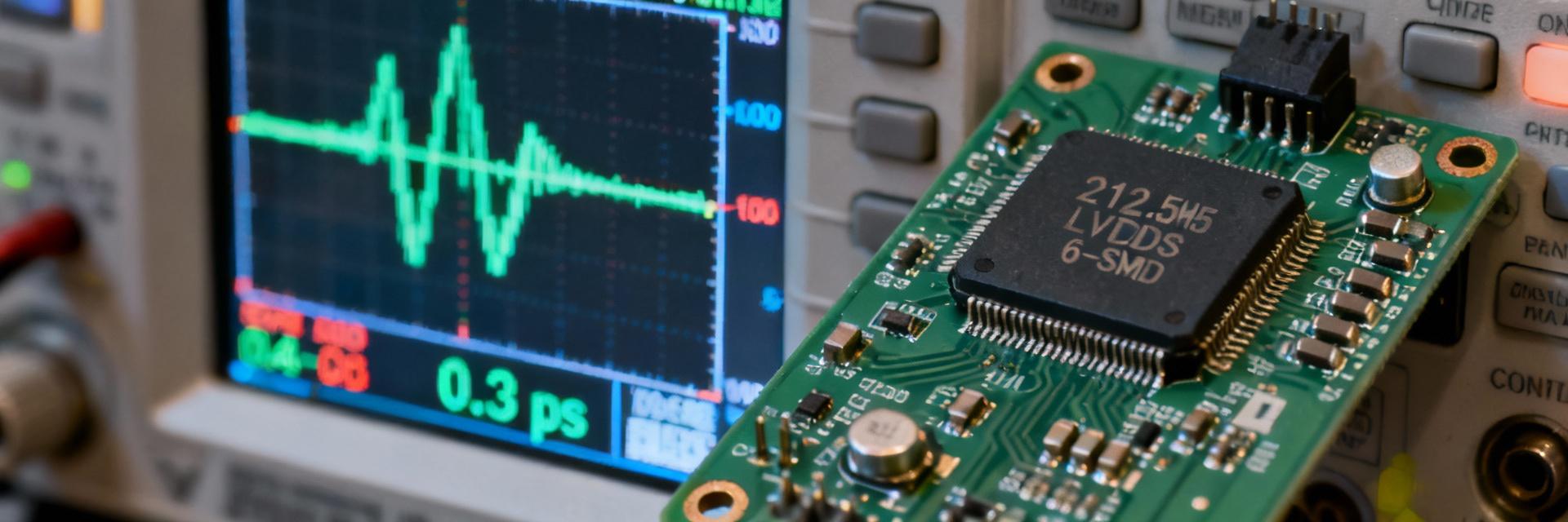
Sample testing is the final gate for validating selection. Use high-impedance probes to measure the clock waveform and observe rise/fall times. For high-speed applications, evaluate jitter through eye diagrams and check for spurs using a spectrum analyzer. Choose reputable suppliers and clarify consistency requirements for full-temperature range testing before bulk purchasing.
Key Summary
Requirements First
Precise matching begins with a clear definition of scenarios, accuracy, jitter, and voltage load.
Interface Matching
Understand CMOS characteristics, accurately calculate load capacitance, and optimize PCB layout.
Long-term Stability
Evaluate stability across the full temperature range and aging rates to ensure high-reliability applications.
Verification Loop
Lock in quality suppliers and guarantee mass production through eye diagram and spectrum analysis measurements.
Frequently Asked Questions
How to quickly determine if a 33.333MHz CMOS oscillator matches my MCU?
Check three basic parameters: first, the supply voltage must be identical; second, confirm the MCU requires CMOS levels and level thresholds; third, calculate the required load capacitance value based on the manual's recommended load circuit and compare it with the oscillator's nominal value. It is recommended to perform full-temperature testing in the actual circuit.
Why do I see many glitches on my 33.333MHz clock signal on the oscilloscope?
This usually stems from power supply noise or improper measurement. Check if decoupling capacitors are placed close to the pins and use a grounding spring instead of a long ground wire during measurement. If the problem persists, try connecting a resistor of about 33Ω in series at the output to damp overshoot and ringing.
In cost-sensitive projects, what aspects of choosing a CMOS oscillator can be simplified?
Non-critical parameters can be relaxed, such as choosing ±50ppm stability, a 0-70°C temperature range, and universal packaging. However, core functional parameters such as power supply voltage matching and load capacitance cannot be compromised. At the same time, avoid products from unknown sources to maintain basic reliability.
@keyframes grow { from { width: 0; } }
@keyframes fadeInDown {
from { opacity: 0; transform: translateY(-20px); }
to { opacity: 1; transform: translateY(0); }
}
READ MORE


