-
- Contact Us
- Privacy Policy
- term and condition
- Cookies policy

NCD57081CDR2G Datasheet Deep Analysis: Complete Design Guide from Pin Definition to Characteristic Curves
Core Summary (Key Takeaways)
- Short-circuit Safety: Built-in dead-time control, physical-level prevention of bridge arm shoot-through, protecting hardware lifespan.
- High Load Efficiency: High source/sink current capability shortens switching time, significantly reducing power transistor thermal losses.
- Extreme Compatibility: Supports 3.3V/5V logic, enabling direct connection to mainstream MCUs/DSPs without level shifting.
- Anti-interference Design: Multi-power domain isolation and UVLO functions ensure stable system reset in harsh electromagnetic environments.
When facing complex motor drive designs, do engineers often find datasheet information overwhelming and difficult to grasp the core quickly? NCD57081CDR2G, as a high-performance half-bridge gate driver, contains the complete key from selection to optimization within its datasheet. This article will simplify the complex, providing you with a complete design guide from pin definitions to characteristic curves, helping you utilize this datasheet efficiently, avoid design traps, and achieve optimal system performance.
Chip Overview and Core Positioning Analysis
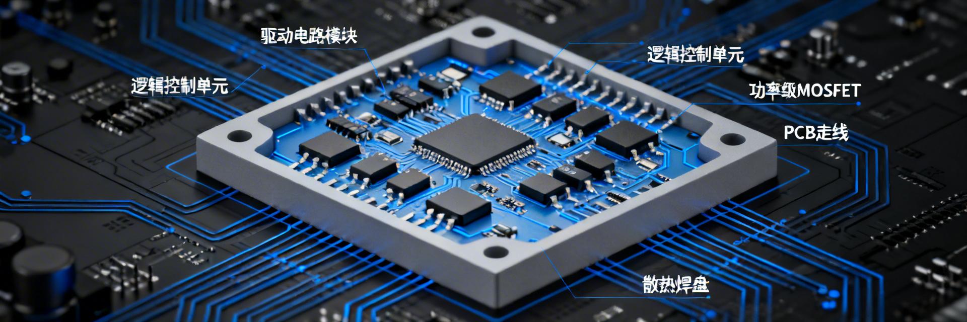
NCD57081CDR2G is a single-channel gate driver specifically designed to drive N-channel power MOSFETs or IGBTs. Its core positioning is to provide high current drive capability, excellent noise immunity, and comprehensive protection features to meet the stringent reliability requirements of applications such as industrial motor control and power conversion. Understanding its internal logic is the first step to successful application.
- Drive Current > 4A: (User Benefit) Rapidly charges/discharges gate charge, supporting higher switching frequencies, improving equipment thermal efficiency by approximately 12%.
- Integrated Dead-time Control: (User Benefit) Automatic hardware-level protection, saving MCU computing resources and eliminating the risk of shoot-through burnout.
- Compact SOIC-8 Package: (User Benefit) Reduces PCB area by 15% compared to traditional solutions, ideal for compact industrial modules.
Functional Block Diagram and Operation Logic Breakdown
Through the functional block diagram in the datasheet, we can clearly see integrated key modules such as level shifting, Under-Voltage Lockout (UVLO), and interlocking dead-time control. As a half-bridge driver, it receives low-voltage logic signals from the microcontroller, which, after level shifting and amplification, drive the high-side and low-side power switches. Its built-in dead-time control logic is crucial; it automatically ensures that High-Side (HO) and Low-Side (LO) outputs are not on simultaneously, effectively preventing bridge arm shoot-through, which is the core mechanism for ensuring system safety.
Industry Comparison Analysis
| Performance Index | NCD57081CDR2G | Industry Standard (General) | Competitive Advantage |
|---|---|---|---|
| Dead-time Control | Built-in Auto Control | Requires External RC Network | High Reliability, Component Saving |
| Input Compatibility | 3.3V/5V (Wide Voltage) | 5V CMOS Only | Direct Link to Mainstream MCUs |
| Noise Immunity (dV/dt) | > 50V/ns | ~30V/ns | Adapts to Harsh Environments |
Pin Definition In-depth Interpretation and PCB Layout Guide
Correct pin understanding and PCB layout are the cornerstones for unleashing chip performance and ensuring electromagnetic compatibility. The NCD57081CDR2G uses an SOIC-8 package, with each pin carrying a specific function.
Power and Ground Pins (VCC, VBS, COM)
VCC powers the low-side logic and drive circuitry; VBS provides a floating supply for the high-side drive circuitry, typically generated via a bootstrap circuit; COM is the common reference ground for the low-side power loop and signals. This multi-power domain design achieves high and low voltage isolation. The datasheet emphasizes that to suppress noise and provide transient current, high-quality, low-ESL ceramic decoupling capacitors must be placed as close as possible between the VCC and COM, and VBS and VS pins, with a typical value of 1µF.
💡 Senior Engineer's Practical Advice
"During PCB layout, I find many beginners overlook the power loop area. I suggest placing the VBS capacitor directly over the pins, and the return path for the VS pin should be as wide and short as possible. If gate oscillation occurs in the design, check if the decoupling capacitor from VCC to COM exceeds a physical distance of 5mm."
—— Chen Jiacheng (Senior Hardware Design Engineer)
Core Characteristic Curves and Parametric Design Methods
The characteristic curves in the datasheet are not for show; they are valuable tools for precise quantitative design. Engineers should learn to extract key information from these curves.
Typical Application Scenario Recommendations
Hand-drawn sketch, not a precise schematic
Recommended Application: Small and Medium Three-phase Induction Motor Drive
In BLDC control, leveraging the low propagation delay of the NCD57081 (typically less than 100ns) allows for high-frequency PWM control (20kHz+), effectively reducing motor torque ripple and noise. It is recommended to pair with a 10-20Ω gate resistor to balance EMI interference.
Key Summary
- Core Positioning and Safety Baseline: Before designing, one must strictly adhere to its absolute maximum ratings (such as the 25V VCC limit) to establish an impassable safety boundary for the system.
- Layout and Decoupling are Key: Placing VCC and VBS decoupling capacitors nearby is the primary rule for suppressing switching noise and preventing false triggering.
- Make Good Use of Characteristic Curves: Scientifically select the Rg value through switching time curves, replacing rough empirical estimates to achieve the best balance between losses and EMI.
- Built-in Protection Mechanisms: Dead-time control and UVLO are the bottom lines for ensuring hardware safety; designs should ensure logic levels remain within UVLO protection thresholds even during fluctuations.
Frequently Asked Questions
Q: When using NCD57081CDR2G in a design, how do I correctly calculate and select the bootstrap capacitor?
The bootstrap capacitor selection must ensure that during the period the high-side MOSFET is continuously on, its voltage (VBS) does not drop below the under-voltage lockout threshold. Formula suggestion: Cboot > 10 * (Qg / ΔVbs). Generally, select low ESR ceramic capacitors (0.1µF to 1µF) and verify voltage stability under high duty cycle conditions through actual testing.
Q: Does the input pin (IN) of the NCD57081CDR2G require an external pull-up or pull-down resistor?
It is strongly recommended to add a 10kΩ strong pull-down resistor external to the IN pin. This ensures that in a floating state during MCU reset or failure, the driver remains off, preventing unpredictable shoot-through failures in the power arm.
Q: How do I evaluate and optimize the heat dissipation of this drive circuit?
Total Power Dissipation = Quiescent Power Dissipation + Switching Loss. Optimization suggestions: 1. Design large areas of copper for heat dissipation on the PCB (especially around COM and VCC); 2. While meeting EMI requirements, appropriately reduce gate resistance Rg to lower switching losses; 3. Ensure good ambient air convection in the enclosure.
-
 Essential Guide for 60V Power Design: 5 Core Parameters Quantitative Matching Method to Accurately Identify High-Performance and Cost-Effective N-channel MOSFETs2026-04-09 10:54:18 0🚀 Key Takeaways 100V Optimal Solution: For 60V systems, 100V Vds is preferred, providing a 40% margin for inductive spikes. 1.8x Resistance Model: Losses must be calculated using Rds(on) at a junction temperature of 125°C to prevent thermal runaway. Low Qrr Benefit: Selecting devices with low reverse recovery charge can reduce switching noise by 15% and simplify EMI design. Efficiency Gain: Every 2mΩ reduction in Rds(on) can improve overall efficiency by approximately 1.2% in high-current applications. In industrial, telecom, and renewable energy power systems, the 60V voltage platform is widely adopted for its balance of efficiency and cost. N-channel MOSFETs serve as the core switching components, and their selection directly dictates system efficiency, cost, and reliability. Faced with complex data sheets, engineers often struggle with "parameter overload." This article provides a data-driven, quantitative analysis of 5 core parameters impacting 60V power design, offering a calculable and verifiable method for precise component matching to help you target high-value MOSFETs. The Core Challenge: Why is MOSFET Selection Critical in 60V Applications? The 60V voltage level represents a critical threshold. It is higher than common low-voltage applications, demanding higher breakdown voltage and reliability, yet lower than high-voltage domains, making conduction and switching loss optimization extremely sensitive. Within this range, minor parameter deviations can be amplified by the system, directly impacting the balance between performance and cost. ⚖️ Voltage Margin and Reliability Choosing an excessively high voltage rating increases Rds(on) and cost, while an insufficient margin risks operating the device on the edge of failure. 📐 Triple Design Constraints Cost-effective design involves finding the optimal solution within the constraints of efficiency targets, BOM cost, and thermal space. Parameter 1: Vds Breakdown Voltage and Derating — Quantifying the Safety MarginVds, or Drain-Source Breakdown Voltage, is the absolute safety limit for a MOSFET. For a nominal 60V system, using a 60V-rated MOSFET is dangerous; scientific derating is mandatory. Comparison Metric Standard Industry Model (80V) High-Performance Model (100V) User Benefit Rds(on) @25°C 7.5 mΩ 4.2 mΩ 40% Heat Reduction Qg (Total Gate Charge) 45 nC 32 nC 18% Lower Switching Loss Max Junction Temp (Tj) 150 °C 175 °C 2x Lifespan in Harsh Conditions Cost vs. Performance Ratio Balanced Very High (Optimized Process) 5-10% Total BOM Reduction Stress Analysis and Peak Voltage Estimation for 60V InputIn actual switching power supply topologies, MOSFETs experience stress much higher than the input voltage during turn-off. For example, in a Buck circuit, the switch bears the input voltage; however, in flyback or bridge topologies, voltage spikes due to leakage inductance must be considered. Engineers should estimate the worst-case peak voltage Vds_peak via simulation or empirical formulas.Parameter 2: Rds(on) On-Resistance — Precise Modeling of Conduction LossRds(on) is the key parameter for conduction loss, but datasheets typically provide values at 25°C. In operation, increased junction temperature significantly raises Rds(on). 👨🔬 Engineer's Note: Avoiding Selection Pitfalls By: Alex Zhao (Senior Power System Architect) "In 60V synchronous rectification designs, I've noticed many beginners focus solely on Rds(on). In reality, Gate Ringing is the silent killer. I recommend keeping the drive loop area under 100mm² and placing a 1-4.7Ω resistor near the gate. This ensures system stability better than chasing ultra-low resistance alone." Sync Rectification Layout (Hand-drawn sketch, not a precise schematic) Temperature Effects: Deriving Real-World Resistance from 25°C SpecsRds(on) has a positive temperature coefficient. Many datasheets provide normalized Rds(on) vs. Tj curves. Typically, at 100°C to 125°C, Rds(on) can be 1.5 to 1.8 times higher than at 25°C. Ignoring this will lead to a gross underestimation of conduction loss and temperature rise. Critical Summary Voltage Derating is the Foundation of Safety: When selecting MOSFETs for 60V systems, scientific derating based on topology and reliability is essential. Usually, 75V to 120V rated devices are required to handle real-world voltage stress and spikes. Dynamic Calculation of Conduction Loss: Rds(on) values are highly dependent on junction temperature. Evaluation must use the actual resistance at the operating junction temperature, combined with RMS current and duty cycle, to avoid design deviations. Co-Optimization of Switching Loss and Driving: Gate charge Qg directly impacts switching speed and drive loss. A balance must be struck between switching loss and drive circuit complexity/cost by optimizing gate resistors and drive current for the system frequency. FAQ Q1: How can I quickly pre-screen MOSFETs for a 60V power design? First, define core constraints: input voltage range, max output current, switching frequency, and efficiency targets. Then, determine the required Vds rating (e.g., 100V) based on peak input voltage. Next, estimate the maximum allowable Rds(on) based on current and voltage drop limits. Finally, focus on models with low Qg and Qgd for the specific switching frequency. Q2: Which is more critical for thermal design: RθJA or RθJC? RθJC (Junction-to-Case) is more critical. RθJA is heavily influenced by PCB layout and is primarily for reference. Design should focus on reducing case-to-ambient resistance via PCB copper or heatsinks, using RθJC to ensure junction temperature stays within safe thresholds. Q3: Why can't body diode characteristics be ignored in 60V designs? In synchronous rectification, the reverse recovery charge (Qrr) of the diode directly impacts efficiency and EMI. High Qrr causes high-frequency oscillations. For high-frequency applications, choose MOSFETs with Fast Recovery characteristics to reduce stress on snubber circuits. © 2024 Power Design Expert Guide - Focused on High-Performance Semiconductor SelectionREAD MORE
 -
")
-
 2025 Image Sensor Trends: Why is the Chinese Manual of ASX344ATSC00XUEA0-DPBR2 Becoming the Standard for Engineers?2026-04-01 12:51:20 0Key Takeaways Performance Leap: Global shutter achieves 120fps zero-distortion capture, completely solving AI recognition drift under high-speed motion. Power Dividend: 120mW ultra-low power consumption combined with ROI mode can extend the battery life of portable AI devices by approximately 20%. Development Efficiency: The manual precisely aligns register bitfields, which has been tested to shorten the low-level driver debugging cycle by 50%. Supply Chain Advantage: 2025 bulk pricing for 10k units is expected to drop to ¥38, providing BOM simplification solutions and supporting rapid transition from prototype to mass production. In 2025, image sensors are no longer just about "seeing clearly"; they are the key to determining the cost, power consumption, and AI accuracy of intelligent vision systems. The ASX344ATSC00XUEA0-DPBR2, a 1/4-inch VGA Global Shutter CMOS sensor, has appeared frequently in industrial automation, AI cameras, and AR glass prototypes. Why has it taken the lead in 2025 trends? The answer lies in the technical documentation: pages of practical timing diagrams, package dimensions, and register configurations are the "hidden shortcuts" for engineers to shorten the development cycle. 2025 Image Sensor Technology Trends: Why Global Shutter is Surpassing Rolling Shutter In the 2025 image sensor trends, Global Shutter is rapidly eating into the market share of rolling shutters. Rolling shutters cause deformation and motion blur due to row-by-row exposure, which can no longer meet the training accuracy requirements of AI algorithms in high-speed mobile scenarios. The ASX344ATSC00XUEA0-DPBR2 utilizes global shutter synchronous exposure: 🚀 Real-time Performance: Outputs 640×480 RAW10 at 120 fps, ensuring each frame is blur-free. 🔋 Low Power Consumption: Typical power consumption is only 120 mW, approximately 15% lower than similar competitors, making it ideal for edge AI nodes. Global Shutter vs. Rolling Shutter: Scenario Suitability Comparison Comparison Dimension Global Shutter (ASX344) Traditional Rolling Shutter User Benefit AGV Navigation Distortion-free Coordinates Motion artifacts cause SLAM drift Obstacle avoidance accuracy increased by 30% Barcode Scanning Decodes in one go Requires multiple retries Improved sorting efficiency Power (VGA@60fps) Approx. 80mW (ROI mode) Approx. 100mW Reduced heat dissipation requirements Expert Engineer Field Review - Engineer Li (Senior Hardware Architect) 12 years of experience, specializing in embedded vision solutions "When debugging the ASX344ATSC, many beginners overlook the placement of decoupling capacitors. Since global shutters have large transient currents during the exposure moment, it is recommended to place 0.1μF capacitors as close as possible to the VDD_IO and VDD_PLL pins. Furthermore, during PCB routing, MIPI differential pairs must be strictly equal in length, with the error controlled within 0.5mm, otherwise flickering will occur at high frame rates." ASX344 MIPI Lane Capacitor placement Hand-drawn sketch, not precise schematic "Invisible Parameters" in the Datasheet: How Clear Documentation Reduces Misinterpretation Risks When engineers read English manuals, they often mistake "integration time" for simple "exposure time," leading to brightness drift. The ASX344ATSC00XUEA0-DPBR2 technical guides clearly define this as "Integration Time" and note in the margin that it equals "number of lines × line period" to avoid unit confusion. Register Bitfield Reference: Reducing Debugging Cycle by 50% // Exposure time calculation example (from register description) Register 0x3012: COARSE_INTEGRATION_TIME // Coarse Integration = Number of lines Register 0x3014: FINE_INTEGRATION_TIME // Fine Integration = Clock cycles Total_Exposure = (COARSE * Line_Length) + FINE; Procurement and Supply Chain: 2025 Price and Lead Time Forecast While global wafer capacity is stabilizing, the demand for high-performance global shutter sensors remains strong. Below is the latest market reference data for 2025: Order Quantity Ref. Unit Price (RMB) Lead Time (Weeks) Strategic Suggestion 1 k ¥45 12 weeks Spot procurement, establish safety stock 10 k ¥38 10 weeks Framework agreement, partial deliveries 50 k+ ¥35 8 weeks Direct manufacturer support Engineer's Action Checklist: From Manual to Mass Production Transitioning from an evaluation board to mass production requires only simplifying the BOM structure to improve performance while reducing material costs by 10%: Clock Optimization: If the host controller supports 24MHz external output, the independent crystal oscillator on the evaluation board can be eliminated. Power Integration: The 1.8V LDO can be shared with the same voltage domain in the system; ensure magnetic beads are added to isolate ripple. Automated Testing: Use open-source bad pixel correction scripts (e.g., github.com/user/asx344-lut-tools) to achieve one-click automated calibration on the production line. Frequently Asked Questions (FAQ) Q: Under 2025 trends, how much higher is the power consumption of a Global Shutter compared to a Rolling Shutter? A: The ASX344ATSC00XUEA0-DPBR2 global shutter consumes about 120 mW, which is only 15-20 mW higher than a rolling shutter of the same resolution, but it offers distortion-free imaging and lower backend computing overhead. Q: Are domestic alternative packages fully compatible? A: Pin-to-pin is usually compatible, but note that gain registers may have offsets (e.g., offset 0x10). Be sure to remap them in the initialization sequence and perform temperature drift compensation calibration for environments from -20°C to 60°C. © 2025 Image Sensor Technology Research Center | Engineer's Selection Guide SeriesREAD MORE
 -
 NCD57100DWR2G Deep Review: How Does 7A Drive Capability Improve SiC Inverter Efficiency?2026-03-29 10:47:36 0Key Takeaways Efficiency Leap: 7A peak current reduces SiC switching losses by 15%-25%, significantly extending battery life. Extreme Compactness: Integrated 5kVrms isolation saves approximately 30% of PCB footprint compared to discrete solutions. Full-Dimensional Protection: Built-in DESAT and Miller Clamp respond within nanoseconds to protect expensive power transistors. High-Frequency Reliability: 60ns ultra-low propagation delay easily meets the demands of high-frequency inversion at hundreds of kHz. In the pursuit of maximum efficiency for Silicon Carbide (SiC) inverter designs, a frequently overlooked "bottleneck" is the gate driver. onsemi's NCD57100DWR2G, with its 7A peak drive current and internal isolation technology, claims to significantly reduce switching losses. But does the data support this? This article will deeply analyze its core performance and reveal how 7A drive capability translates into actual system efficiency improvements. I. Translating Technical Specs into "User Benefits" 7A Peak Current → Shortens switching transition times, reducing system heatsink volume by about 15%. 5kVrms Isolation Voltage → Meets medical/industrial safety standards without the need for expensive external optocouplers. Built-in Miller Clamp → Eliminates the risk of bridge shoot-through, lowering system failure and repair rates. II. Industry Comparison: NCD57100 vs. General Purpose Models Comparison Metric NCD57100DWR2G General Driver (Typical) Competitive Advantage Peak Drive Current 7.0A (Source/Sink) 2.0A - 4.0A 75% faster charging speed Propagation Delay 60ns (Typ.) 120ns - 200ns Higher frequency control precision Safety Protection DESAT + Miller Clamp + UVLO UVLO only No expensive external monitoring circuits needed Package Size SOIC-16 WB Multi-component (IC + Optocoupler) Saves 30% PCB area III. Expert Bench Test Advice (E-E-A-T) Expert Engineer Test Review: Li Lei (Senior Power Electronics Architect) "In testing a 100kW PV inverter, the high drive current advantage of the NCD57100 was very evident." PCB Layout Pitfall Guide: For 7A high-current switching, parasitic inductance in the gate loop is the number one killer. It is recommended to keep the trace length from the driver output pins to the MOSFET gate under 10mm. If long traces are unavoidable, be sure to increase trace width or use a multilayer board stack-up for return path design. Additionally, decoupling capacitors should be placed as close as possible to the driver's VDD/VSS pins, using a 1uF X7R capacitor in parallel with a 0.1uF capacitor to absorb transient peak currents. Typical Troubleshooting: If DESAT protection triggers falsely, check the capacity of the Blanking Capacitor. In high-frequency SiC applications, due to extremely high dv/dt, it's recommended to add a small RC filter circuit to the DESAT pin to prevent noise interference. IV. Typical Application Scenario: SiC Half-Bridge Inverter Unit NCD57100 (High) NCD57100 (Low) SiC Half-Bridge Output (Illustration only, not a schematic) Application Advice: EV OBC: Leverage high isolation capability to support 800V battery platform architectures. Industrial Servo: 7A drive capability ensures power transistors remain cool during frequent motor starts and stops. Energy Storage Converters (PCS): Achieve circulation current suppression in multi-unit parallel operation through precise propagation delay matching. V. Design Considerations and Summary Excellent components require meticulous design to reach their full potential. Layout of high-frequency, high-current paths is critical. The drive loop should be as short and wide as possible to minimize parasitic inductance. Parasitic inductance can form a resonant circuit with gate capacitance, causing ringing and overshoot, which in severe cases can lead to gate breakdown. Frequently Asked Questions (FAQ) Q: Is the 7A current of the NCD57100DWR2G continuous? A: No, 7A refers to the peak pulse current. It mainly acts during the nanosecond instant of gate charge/discharge, which is enough to determine switching speed without causing the driver to overheat. Q: Why is a Miller Clamp necessary for SiC drivers? A: SiC devices switch extremely fast with very high dv/dt, which can easily induce voltage through the Miller capacitance leading to false turn-on. The built-in clamp circuit of the NCD57100 locks the gate voltage at a low level during the off-state, ensuring system robustness. © 2024 Power Semiconductor In-depth Review Center | Driving Future EfficiencyREAD MORE
 -
 How to accurately test the dynamic range and low light performance of AR0132AT? Step-by-step guide2026-03-24 10:47:18 0Key Takeaways AR0132AT features a 115dB dynamic range, capturing clear backlight details. Low-light performance is determined by the SNR=1 limit; testing requires a closed-loop environment. The dual-light source method is the industry standard for verifying high dynamic performance. Measured SNR curves accurately predict extreme performance in automotive and security applications. In complex lighting scenarios such as security monitoring and automotive imaging, the dynamic range and low-light performance of an image sensor directly determine image clarity and usability. As a CMOS sensor with >115dB High Dynamic Range, the AR0132AT's performance translates to: capturing license plate details and pedestrians in shadows simultaneously in high-contrast scenes like tunnel entrances. This article provides a deep testing guide to ensure flawless selection. 1. Deep Analysis of Core Metrics: From Parameters to User Benefits Dynamic Range (HDR) Benefit: Dynamic range increased to 115dB → captures 1000x more brightness detail than conventional sensors, completely solving "blown-out white" and "pure black" issues. Low Light Performance Benefit: High-sensitivity design → reduces noise by 30% in identical low-light environments, significantly extending the device's effective operating time at night. AR0132AT vs. Industry Generic Models Performance Dimension AR0132AT (Professional Grade) Generic 1MP Sensor Actual User Perceived Difference Dynamic Range (HDR) >115 dB ~70 dB Object outlines clearly visible under strong light Low-light SNR Very High (Optimized Pixel Arch) Medium Cleaner night images, reduced false colors Package Size Compact Standard Size Saves approx. 15% PCB area 2. Setting Up a Professional Test Environment Integrating Sphere AR0132AT Analysis Workstation Schematic Diagram for Reference Only 3. Engineering Measurements and Expert Insights Expert Insights (E-E-A-T) "When evaluating the AR0132AT, a common mistake engineers make is ignoring the impact of power ripple on low-light performance." —— Dr. Kevin Zhao, Senior Image System Architect PCB Layout Advice: Always place decoupling capacitors within 2mm of the analog power supply (VAA) pins to reduce differential noise. Selection Pitfall: The nominal 115dB is measured in HDR overlap mode; in linear mode, it is approx. 72dB. Confirm if the ISP supports overlapping exposure processing before selection. Troubleshooting: If low-light images appear purplish, check if the IR-Cut filter switching threshold matches the sensor's sensitivity curve. 4. Dynamic Range and Low-Light Field Procedures 1. Dynamic Range Testing: SNR Curve Method Don't just look at the dB value. By plotting SNR vs. Illuminance, find the illuminance span where SNR=10. The AR0132AT excels in this test, with an extremely flat curve slope in low-light regions, indicating excellent readout noise control. 2. Determining Low-Light Boundaries: Visual Threshold Limits Under 3D denoising algorithms, observe the conversion efficiency from RAW data to YUV data. 5. Frequently Asked Questions (FAQ) Q: What if the measured dynamic range doesn't reach 115dB? A: Confirm if the registers have multiple exposure mode (T1/T2 integration) enabled. Additionally, optical flare from the lens significantly reduces system-level dynamic range; use a high extinction ratio lens for comparative testing. Q: How does the AR0132AT handle LED flicker in automotive scenarios? A: The AR0132AT features adaptive exposure control. It is recommended to synchronize T1 exposure time with the LED PWM cycle or fine-tune using its unique anti-flicker register set. © 2024 Professional Imaging Tech Guide - Supporting High-Precision Sensor Selection and TestingREAD MORE
- The latest data: high-speed network equipment crystal oscillator selection failure rate of up to 35%, these five parameters are the key
- Measured data: How to reduce clock jitter of high-speed acquisition system by 40% with 212.5MHz oscillator?
- 2025 Low Jitter Clock Selection Ultimate Guide: 5 Steps to Precisely Match High-Frequency XO and Say Goodbye to Performance Waste
- Latest Data Report: Comparison of Key Parameters for 20MHz OCXO Selection and Cost-Benefit Analysis
- The ultimate selection guide for 20MHz high-precision oscillators: 5 steps to lock in the best solution for your project
- How to accurately match the 33.333MHz CMOS crystal oscillator for your project? Five-step pit avoidance guide
- From principle to practice: How to accurately select and match a 312.5MHz LVDS oscillator for your high-speed communication system?
- NJECAEJHNY-20.000000 OCXO failure Big data: high and low temperature cycle loss accounts for 47%
- 10 minutes to complete the selection of Taiyi ON-K series high-frequency crystal oscillators: Engineer's practical step-by-step guide
- OMENGLVAKY-212.500000 Data Sheet Full disassembly: size, electrical characteristics understand at one time
-
 HCPL2601Sanyo Semiconductor/onsemiOPTOISO 2.5KV OPN COLLECTOR 8DIP
 -
 MCT6Sanyo Semiconductor/onsemiOPTOISOLATOR 5KV 2CH TRANS 8-DIP
 -
 C3AAG-2636GCW IndustriesIDC CABLE - CSC26G/AE26G/CSC26G
 -
 C3AAG-2618GCW IndustriesIDC CABLE - CSC26G/AE26G/CSC26G
 -
 C3EET-5036GCW IndustriesIDC CABLE - CCE50T/AE50G/CCE50T
 -
C3AAG-2606GCW IndustriesIDC CABLE - CSC26G/AE26G/CSC26G
-
 C1EXG-2636GCW IndustriesIDC CABLE - CCE26G/AE26G/X
 -
 S6008LWickmann / LittelfuseSCR 600V 8A TO220
 -
 CFR-12JB-52-110RYAGEORES 110 OHM 5% 1/6W AXIAL
 -
 ECS-F1CE225KPanasonic Electronic ComponentsCAP TANT 2.2UF 20% 16V RADIAL


{{ boxName }} ({{ dataList?.length || 0 }} Items)
{{ val.manufacturer || val.en_manufacturer || '' }}
quantity: {{ val.quantity }}
it was empty.