


帮助您节省成本和时间。

为您的货物提供可靠的包装。

快速可靠的交付以节省时间。

优质的售后服务。
新品上市
更多 +


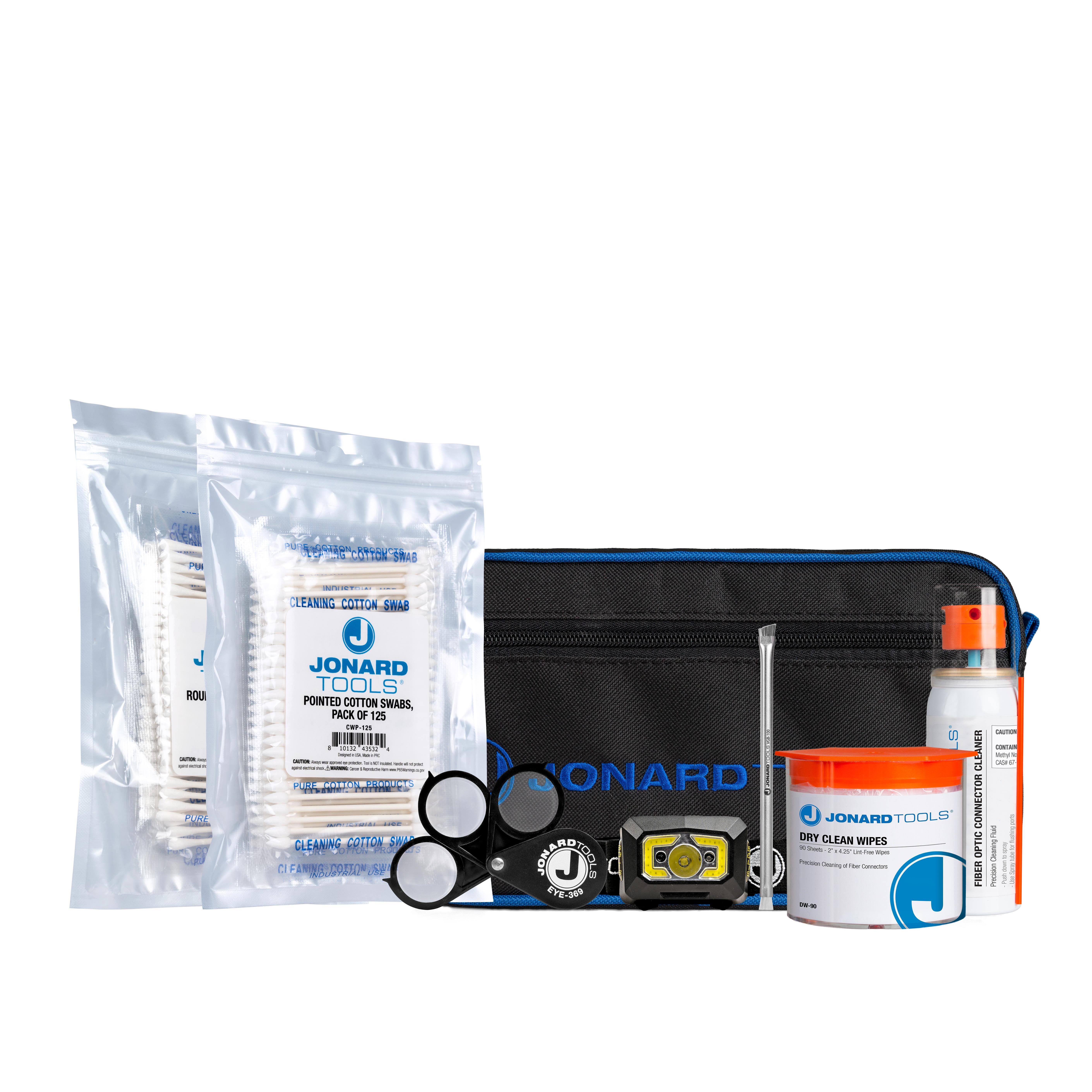


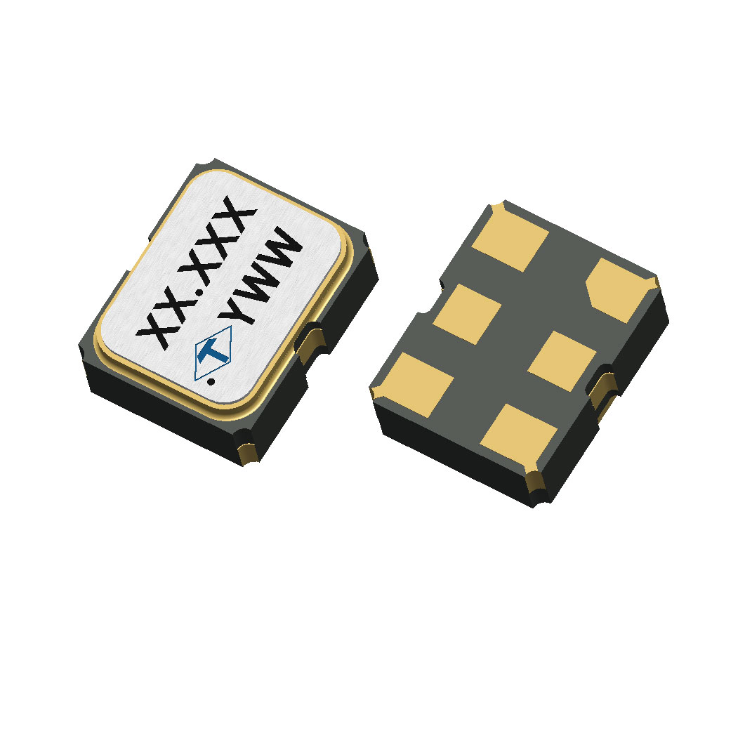
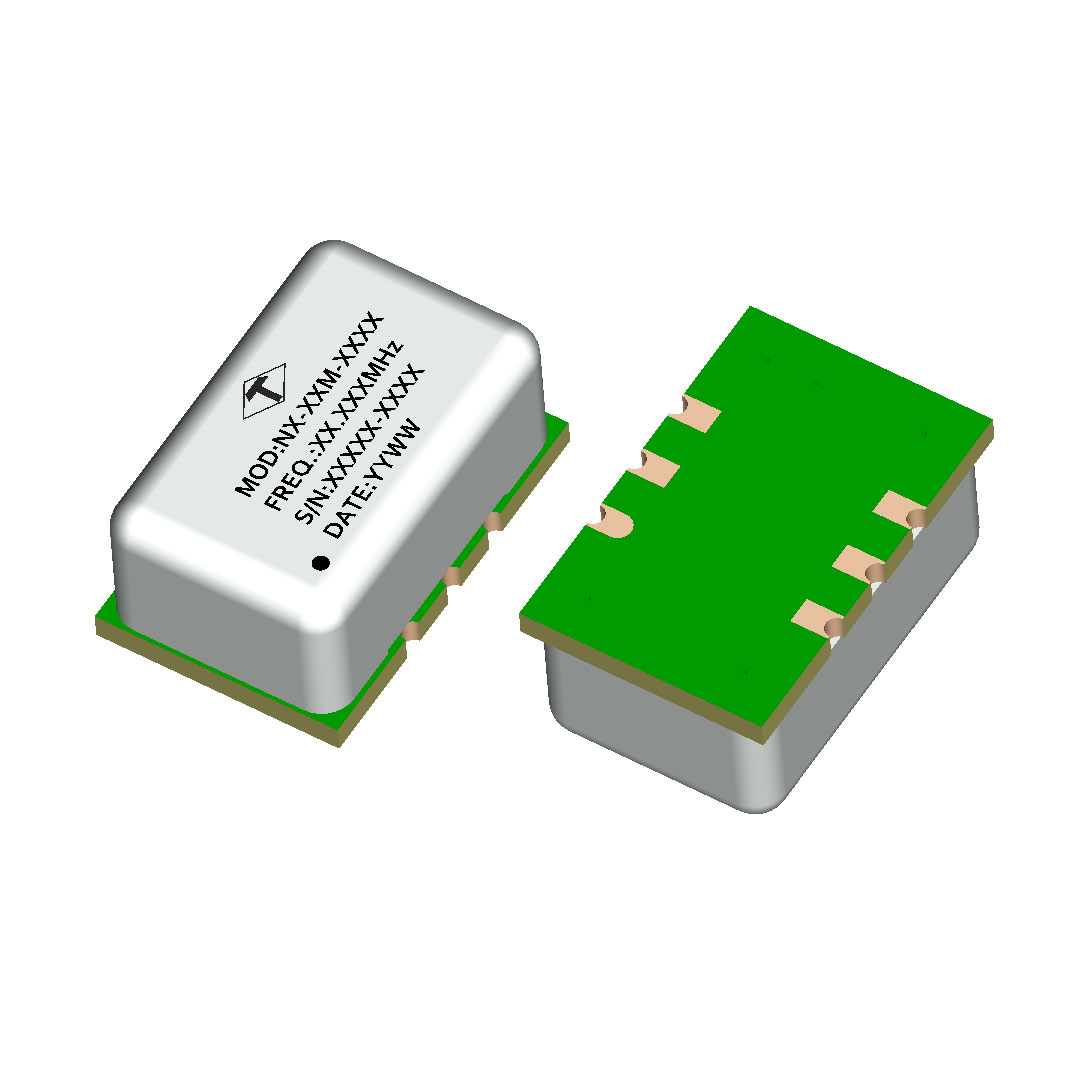
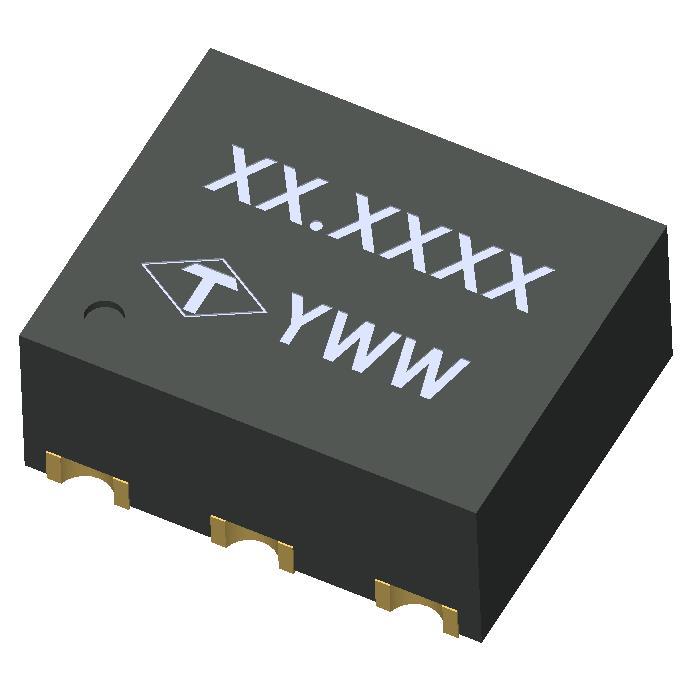
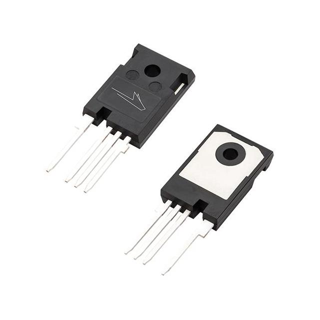
热卖零件


博客
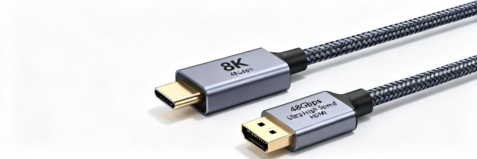
2025年USB-C转HDMI线选购指南:4K与8K画质标准全解析
2025年,随着8K电视出货量突破1500万台,以及4K 144Hz高刷显示器成为电竞标配,一根小小的USB-C转HDMI线,正成为连接移动办公与影音娱乐的刚需。市场上线材价格差异巨大,如何避免买到无法支持4K或8K画质的“假”高速线?本文将为你提供一份硬核选购指南。 USB-C Controller HDMI 2.1 Sink FRL Data Lane (48Gbps) E-Marker Au…
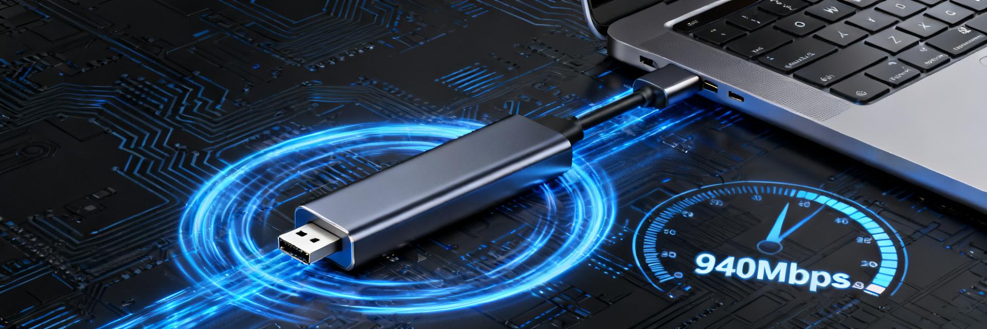
US1GC30B2深度实测:USB-C千兆网卡真实速度对比与兼容性全解析
实测数据显示,市面30%的USB-C千兆网卡实际速率不足标称值的60%。US1GC30B2作为新一代USB-C千兆网卡方案,能否打破"千兆虚标"的行业困局?本文通过实验室级测试数据,还原真实性能表现。 US1GC30B2核心规格与测试环境搭建 USB-C (Host) RTL8153B PHY/MAC Controller RJ45 芯片架构与硬件参数解读 US1GC30B2采用Realtek R…