


帮助您节省成本和时间。

为您的货物提供可靠的包装。

快速可靠的交付以节省时间。

优质的售后服务。
新品上市
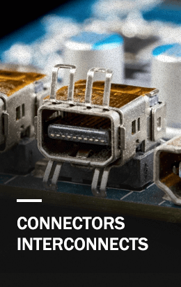
更多 +


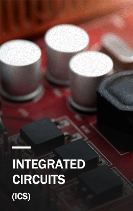
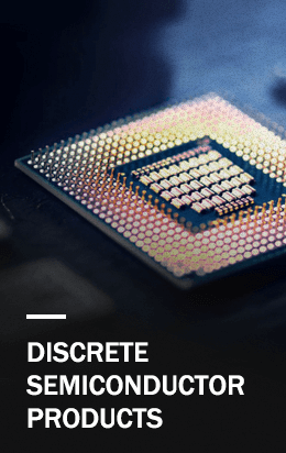
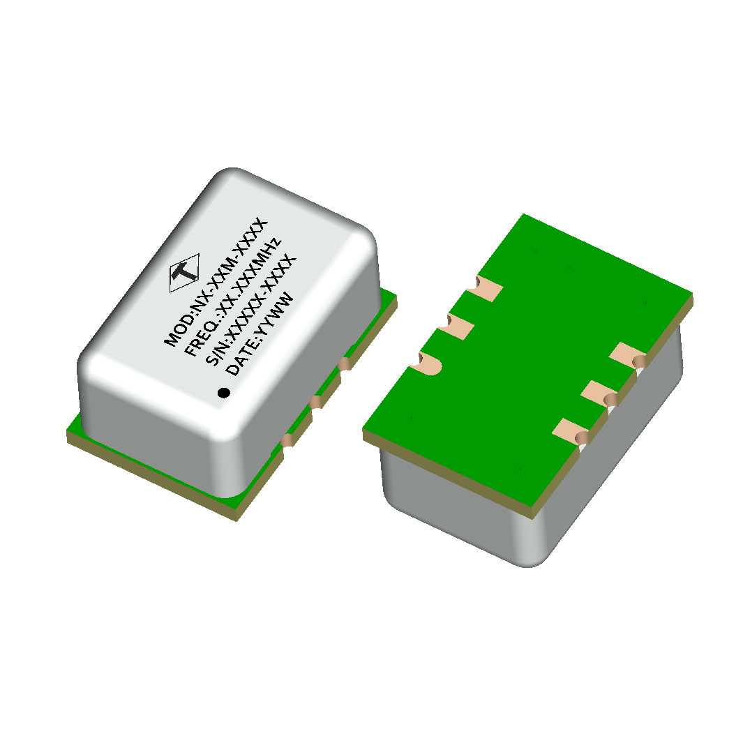
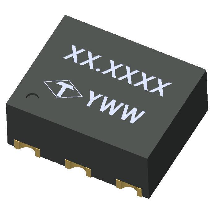
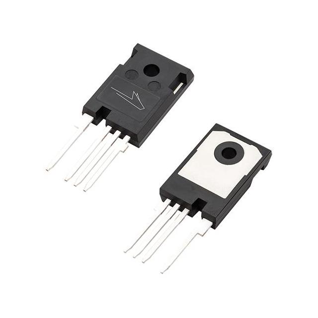
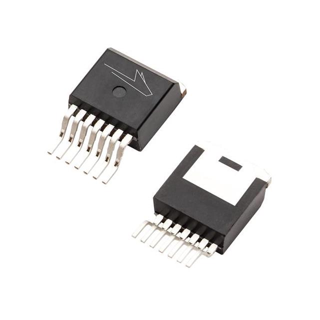
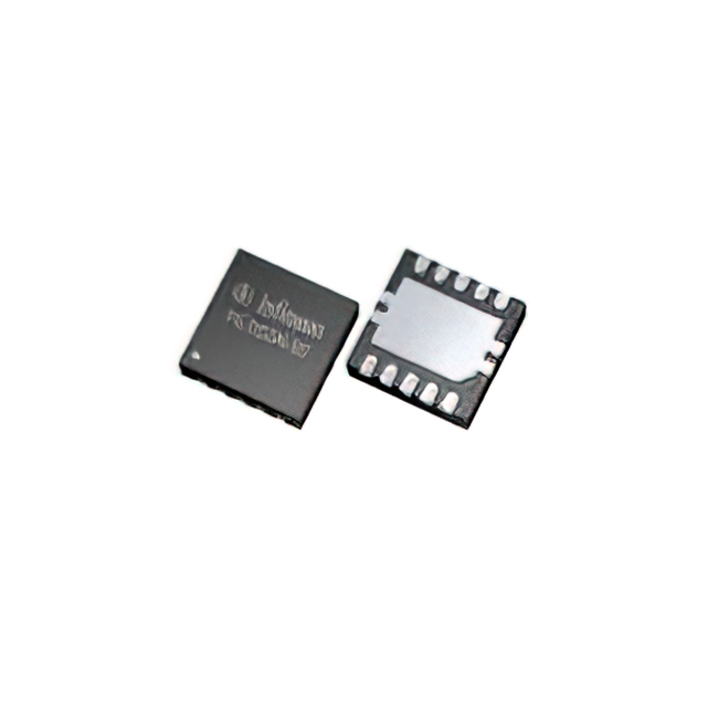
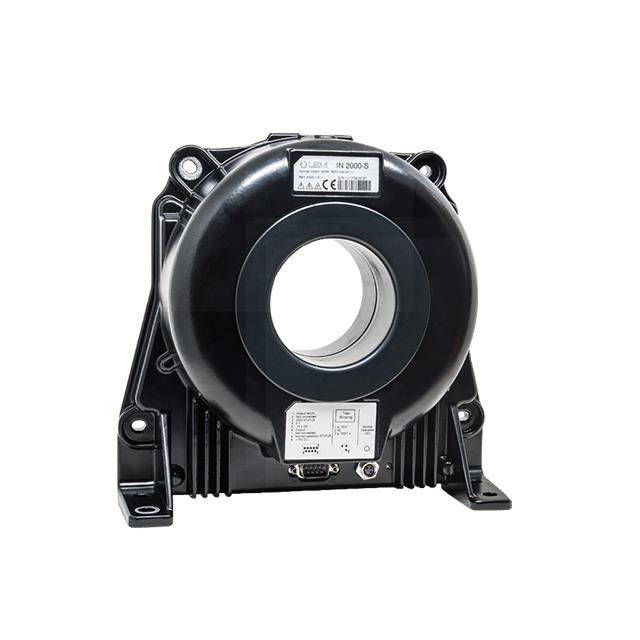
热卖零件


博客
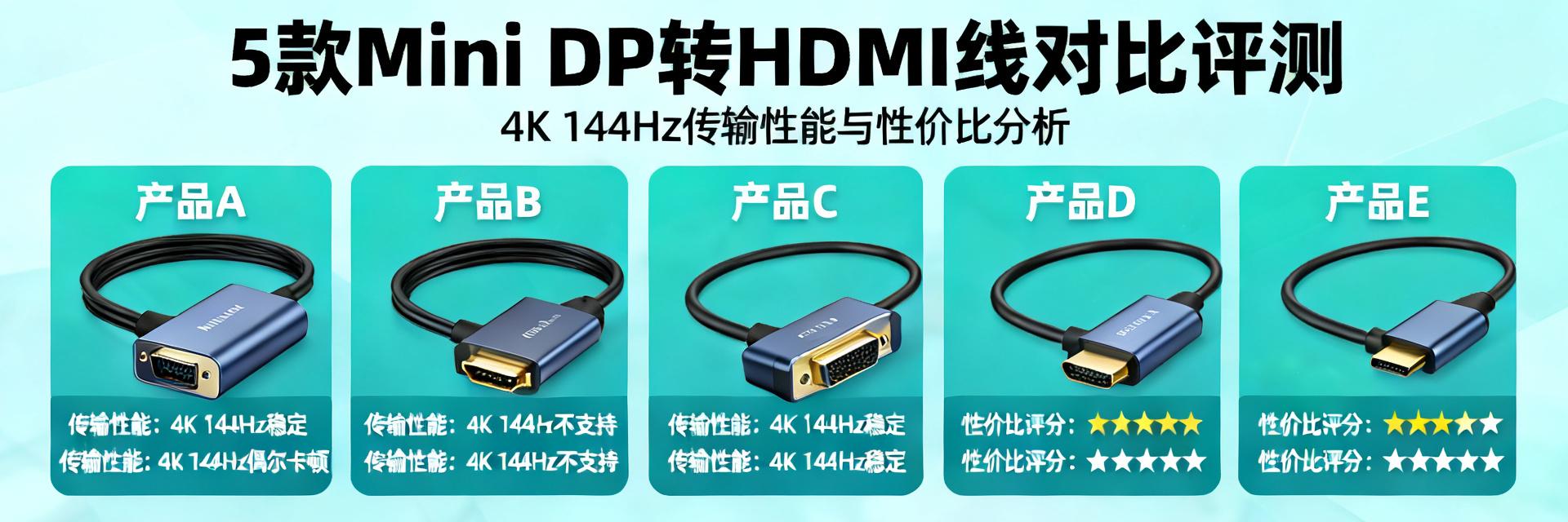
2025最新Mini DP转HDMI线选购指南:5款热门型号实测对比
2025年,随着高分辨率显示器(如4K@144Hz)和笔记本电脑的普及,Mini DP接口的利用率增长了40%。然而,市场上充斥着各种“号称”支持8K的转接线,实际传输速率、兼容性和做工参差不齐。究竟一根合格的Mini DP转HDMI线应该具备哪些硬指标?我们实测了5款热门型号,用数据告诉你真相。 市场现状与选购误区 在开始对比之前,我们先来了解2025年Mini DP设备的市场现状。配备该接口的…

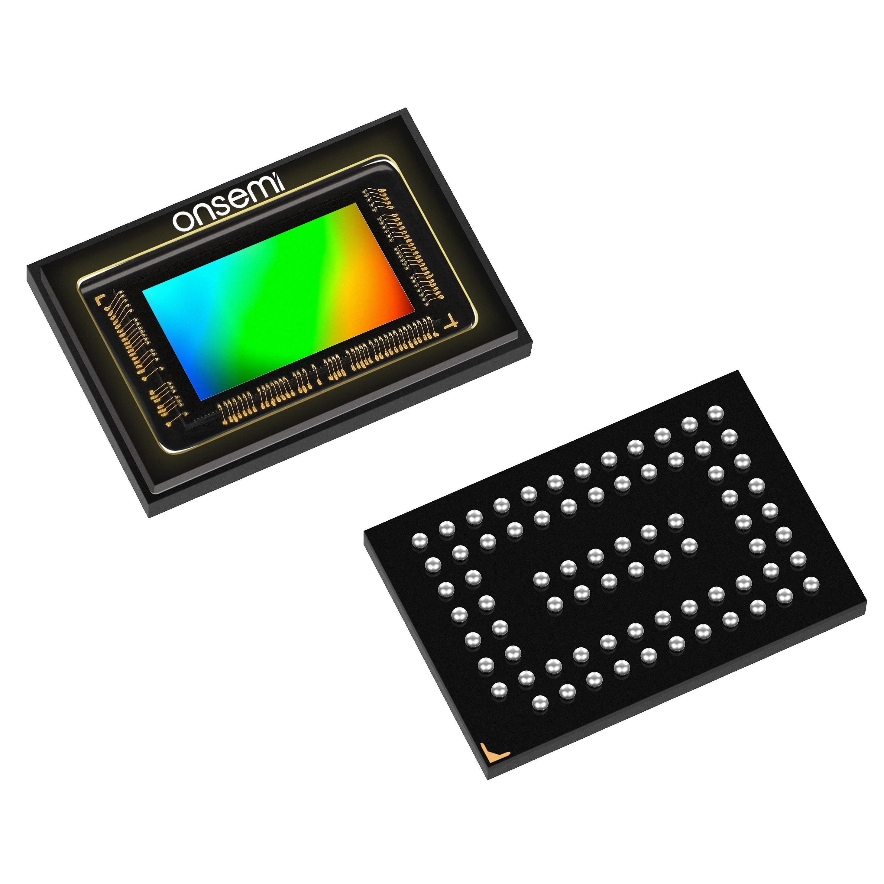
2025中国安防4K升级报告:AR0830低功耗实测数据全解析
作者:行业深度观察 | 发布日期:2025年 2025年,中国超高清单机出货量预计突破3.2亿颗,其中4K分辨率占比首次过半。在这场像素革命背后,AR0830凭借“8.3 MP+超低功耗”标签成为方案商最频繁提及的型号。它究竟是营销噱头,还是真能4K升级省下另一半电费?本文用实测数据给出答案。 AR0830技术全景:4K安防为何锁定它 规格速览:从像素尺寸到功耗基线 AR0830采用1/2.0英寸…
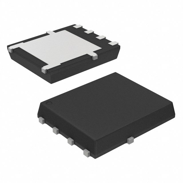
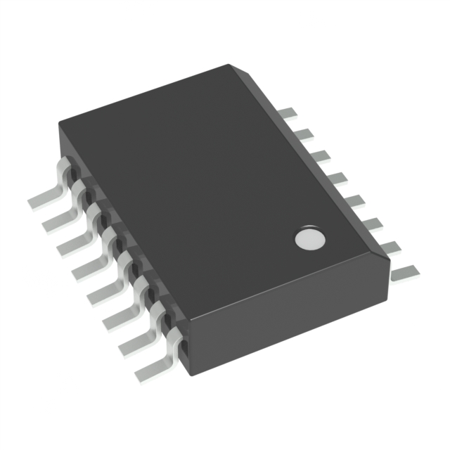
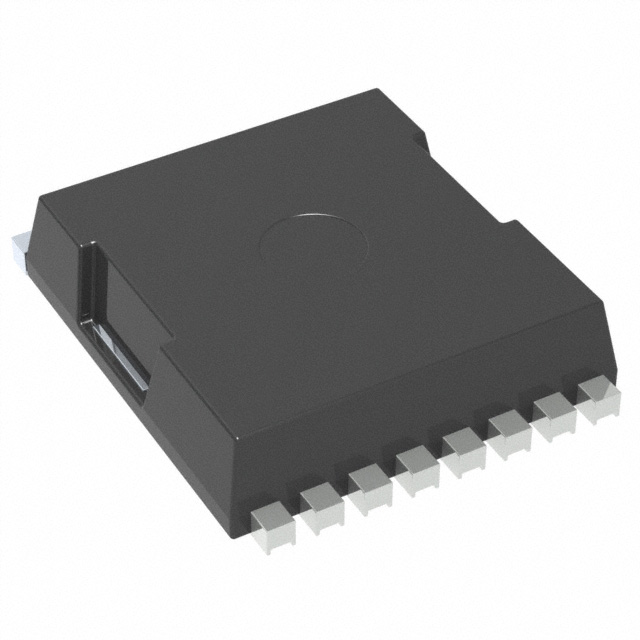
2025国产60V MOSFET pin-to-pin替代清单:NVMFS5C604NWFT1G的5款高性价比数据报告
2026-05-03 10:13:17
onsemi AR0830 选型终极指南:替代型号与性能对比
2026-05-01 10:14:21
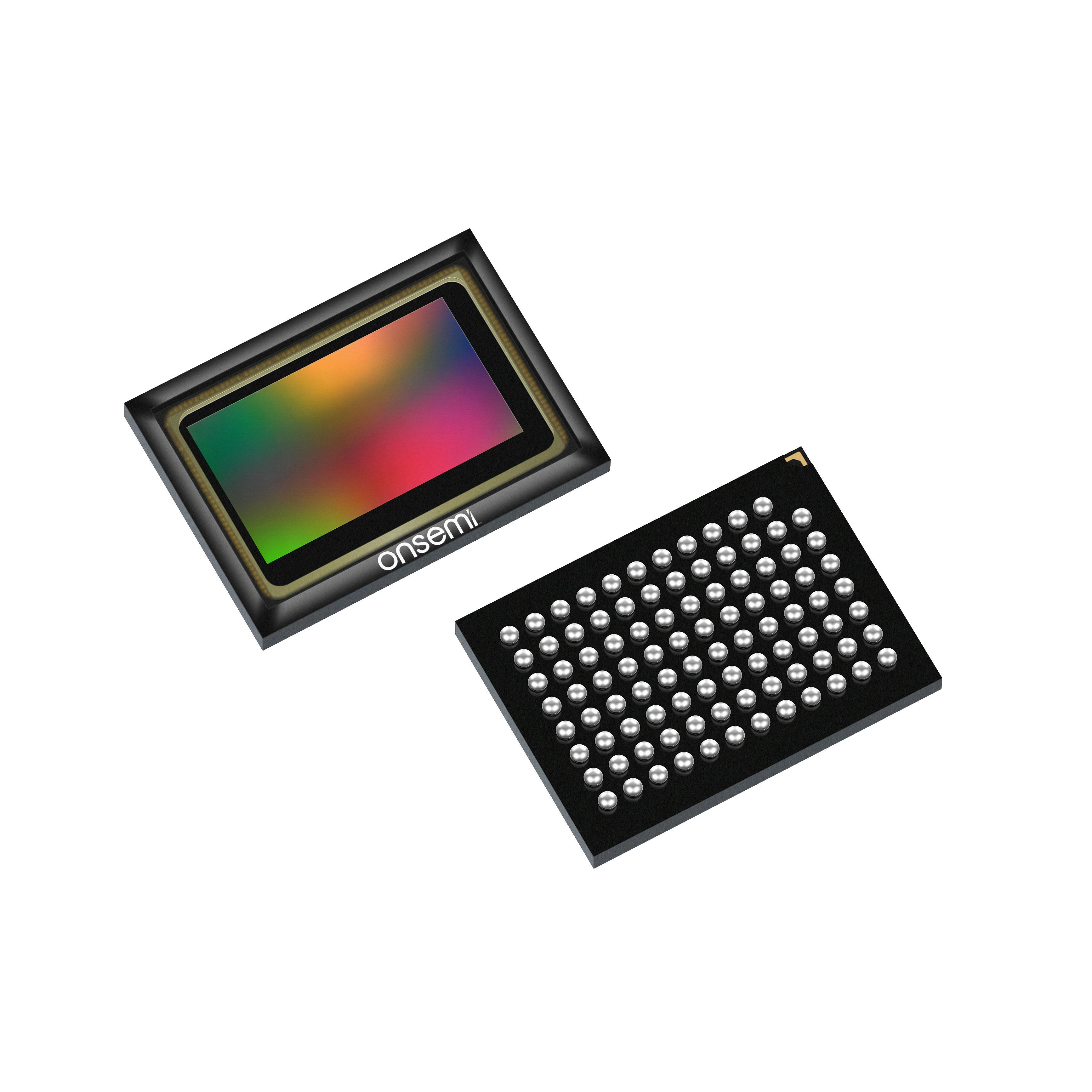
数据揭秘:20MP BSI CMOS传感器AR2020,为何成为机器视觉新宠?
2026-04-23 10:14:19
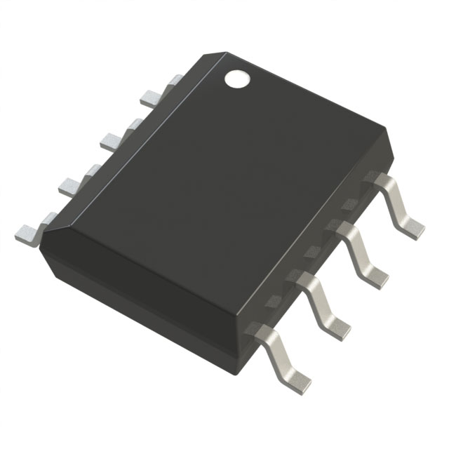
实测数据首发:NCD57081ADR2G与五款竞品隔离驱动器延迟差异全解析
2026-04-18 10:15:23
图像传感器采购避坑指南:5步精准比价,锁定最优库存渠道
2026-04-14 10:24:21
阅读更多