lang.lang_save_cost_and_time
Help you save costs and time.
lang.lang_RPFYG
Provide reliable packaging for your goods.
lang.lang_fast_RDTST
Fast and reliable delivery to save time.
lang.lang_QPASS
High quality after-sales service.
blog
3 February 2026
In 2025, the official LEGO and F1® collaboration series makes a stunning debut. The new City set 60474 "F1 Starting Grid with VCARB & Sauber Cars" has become a focal point for fans due to its unique licensed background and scene design. This article will provide an in-depth analysis of the collectible value of this set. In-depth Analysis of Market Positioning and Pricing Strategy In the LEGO product line, the price per piece is usually an intuitive indicator of value for money. The official pricing for 60474 is approximately €29.99 for 313 pieces, making its price per piece slightly higher than the average for the City series. However, behind this pricing is the significant added value brought by the officially licensed IP. Price Per Piece Comparison (EUR/Piece) LEGO 60474 (F1 Licensed)Approx. 0.096 Regular City SeriesApprox. 0.080 Speed Champions SeriesApprox. 0.110 Exclusive Elements and IP Added Value As a product of the official collaboration between LEGO and F1, 60474 includes the licensed 2025 season liveries for VCARB (formerly AlphaTauri) and the Sauber F1 Team. The collectible significance of this "official certification" is its core value. VCARB Car Accuracy The classic blue, white, and red livery is recreated through fine printed parts and stickers, capturing sponsor logos on the front wing, sidepods, and engine cover. The 8-stud wide body proportions bring the lines closer to the real car. Sauber Car Detail Analysis The green, black, and gold color scheme provides a strong visual impact, perfectly capturing the team's visual identity for the season. For fans seeking a complete team collection, this is an unmissable item. Mini Starting Grid Scene Includes a timing tower that can display qualifying information, red-yellow-green pit lane signals, and starting slots with team logos, simulating a real race weekend. 5 Reasons to Buy for the Core Audience 1 A Low-threshold Entry Point into the LEGO F1 Universe Obtaining two cars from different teams and a scene at an accessible price is an efficient way to experience the charm of LEGO racing. 2 Highly Accurate Team Season Liveries Accurately capturing the team's visual identity for the season, the collectible value becomes more prominent as team results or liveries change. 3 Rich Interactive Features for Simulating Races Operable signal lights and numbered starting slots bring the static model to "life," recreating key moments of the race. 4 Great Potential for MOC Expansion With 313 pieces, there is plenty of room for custom modifications, such as expanding the pit lane, grandstands, or podium. 5 Collectibility and Value Retention: Strategic Debut Status As one of the first sets in the deep collaboration between the City series and F1, it holds high commemorative and forward-looking value for the series. Buying Decision Guide: Recommendations for Target Audiences Characteristic Dimension Performance Rating Recommended Audience Building Difficulty Entry-level (Easy to start) LEGO beginners, youth players Detail Presentation Focused on appearance and livery accuracy F1 team fans, livery collectors Functional Features Scenario-based interaction (signals/slots) Scene enthusiasts, diorama builders Mechanical Structure Minimal (Not Technic style) Not recommended for players seeking complex mechanics Key Summary ● Precise Positioning, IP Value: The highly accurate liveries brought by official licensing are the core value, far exceeding simple price-per-piece calculations. ● Scenario-based Experience, Highly Interactive: The innovative fusion of two race cars and starting grid features significantly enhances the immersion of simulating a race. ● Five Core Drivers: Low threshold, specific team collection, rich playability, MOC potential, and debut value precisely cover core demands. Frequently Asked Questions (FAQ) Is LEGO 60474 suitable for F1 fans who have never built LEGO before? + Very suitable. This set has a moderate piece count (313 pieces) with clear building instructions, and the difficulty is entry-level. At the same time, it includes core elements of F1 racing, allowing beginners to quickly feel the charm of LEGO racing models and F1 culture. How is the value retention of 60474 as a collectible? + LEGO racing theme sets, especially those with clear season characteristics and team-licensed liveries, usually possess certain value retention potential after retirement. As one of the first products in the City F1 series, its long-term collectible value is worth anticipating. Besides display, what other ways are there to play with LEGO 60474? + There are many ways to play. You can use the starting grid scene to simulate a race start; have cars enter and exit the pit lane; and even use it as a base to build larger stands, pit boxes, or a complete track using other bricks you have at home.
LEGO 60474 In-depth Review: Is 313 Granules Worth It? 5 Must-See Purchase Reasons for F1 Racing Fans
2 February 2026
In-depth Industry Field Test Release Date: March 2025 · East China Backbone Network Reconstruction Site Report In March 2025, at the backbone network reconstruction site of a province in East China, using only domestic fusion splicers combined with the TK-285 Cleaning Kit, the average splicing loss plummeted from 0.08 dB to 0.012 dB, a reduction of up to 85%. After the field test report was published, maintenance costs were cut in half. This article will deconstruct the entire process using raw field data. Background Perspective: The Invisible Killers of Optical Fiber Loss As optical fiber networks enter the 400G era, an additional loss of 0.01 dB can instantly strain the link budget. Domestic fusion splicers are often criticized for being "0.02 dB worse than imported ones." The root cause is not the machine itself, but often overlooked contamination: dust, grease, and volatile residues. The Significance of 0.01 dB Level Loss for 5G Bearer Networks 5G fronthaul links are extremely sensitive to budgets; every 0.01 dB of redundancy at each joint accumulates into system-level alarms. The TK-285 cleaning kit compresses the failure rate to a parts-per-million level, meaning a single maintenance session can extend the life cycle of optical cables by 3-5 years. Deep Dive into the TK-285 Cleaning Kit The kit includes 6 lint-free tools covering five major contamination areas: the V-groove, pressure hammer, lens, and fiber end faces of the fusion splicer. The new generation lint-free cloth has a fiber density of 80 g/m², which is 4 times that of traditional cotton swabs, ensuring no shedding and no scratching. Comparison Experiment: New Generation Lint-free Cloth Fiber Density vs. Traditional Cotton Swabs Testing Metrics TK-285 Lint-free Cloth Traditional Cotton Swabs Fiber Shedding Frequency 0 particles/time 12 particles/time Return Loss After Cleaning -55 dB (Excellent) -38 dB (Poor) Time Consumed Per Cleaning 35 seconds 1 min 20 sec Field Test: Three Steps to Reduce Loss by 85% Testing Environment: 25 km trunk line, 1000-core sample, full OTDR recording. Step A Clean objective lens with TK-285 lens cloth Step B Clean V-groove with specialized solvent swabs Step C Unidirectional reciprocating wiping of the end face three times with lint-free cloth Comparison of OTDR curves before and after cleaning shows the average loss dropped from 0.08 dB to 0.012 dB, with statistical significance of P < 0.001. Data Interpretation: Comparison of OTDR Curves Before and After Cleaning "Before cleaning, the curve had a 0.05 dB step at 1.8 km. After cleaning, the step disappeared, and the entire link margin improved by 2.8 dB." —— Field Operation Record of an East China Backbone Network Engineer. Cost-Benefit Actuarial Analysis 1.8 RMB Traditional Maintenance/Core 0.3 RMB TK-285 Maintenance/Core 83% Savings During operator bid evaluation, every 0.01 dB reduction adds 3 points. Using the TK-285 solution directly brings a 5-point competitive advantage. Action Checklist for Frontline Teams 5-Minute Quick Cleaning SOP (Standard Operating Procedure): Power Off: Ensure the device is in a non-electrified cleaning state. Wipe Objective Lens: Gently wipe the optical imaging lens with lint-free cloth. Clean V-groove: Use a specialized swab to remove dust along the groove in one direction. End Face Cleaning: Secondary end face treatment must be performed before the fiber enters the machine. Self-test: Power on to run discharge calibration and self-test programs. Red and Black List of Common Misoperations ✘ Alcohol concentration >99%: Evaporates too quickly, easily leaving dry marks invisible to the naked eye on the lens. ✘ Circular wiping of the end face: Easily creates fine scratches; unidirectional reciprocating wiping should be maintained. 2025 Procurement Trends for Domestic Fusion Splicers Bidding documents have already listed "cleaning compatibility" as a mandatory requirement. It is expected that over 60% of models will come standard with cleaning kits within the year, and the TK-285 is becoming the industry de facto standard. Key Summary Performance Leap TK-285 reduces domestic machine loss by 85%, evidenced by OTDR data. Material Upgrade 80 g/m² lint-free cloth with zero shedding, return loss 17 dB better than traditional tools. Economic Benefits Per-core maintenance cost reduced to 0.3 RMB, a powerful tool for bidding points. Standard Specification 5-minute SOP + inspection sheet, zero-threshold implementation for frontline teams. Frequently Asked Questions Is the TK-285 cleaning kit suitable for all domestic fusion splicers? ▼ Compatible with over 90% of mainstream models, V-groove widths of 1.0-1.6 mm are applicable; verified on-site with various major domestic brands. How long does loss remain stable after one cleaning? ▼ In a standard server room environment, one deep cleaning can stably support about 200 splices; in outdoor dusty environments, it is recommended to perform a quick cleaning every 100 times. Can the lint-free cloth be reused? ▼ Strictly prohibited to reuse. A single lint-free cloth is for one-time use only to avoid cross-contamination. Official advice is to use a clean area of the lint-free cloth for every single fiber core.
2025 The latest TK-285 cleaning kit measured data: the secret of a 85% drop in the loss rate of domestic welding machines
1 February 2026
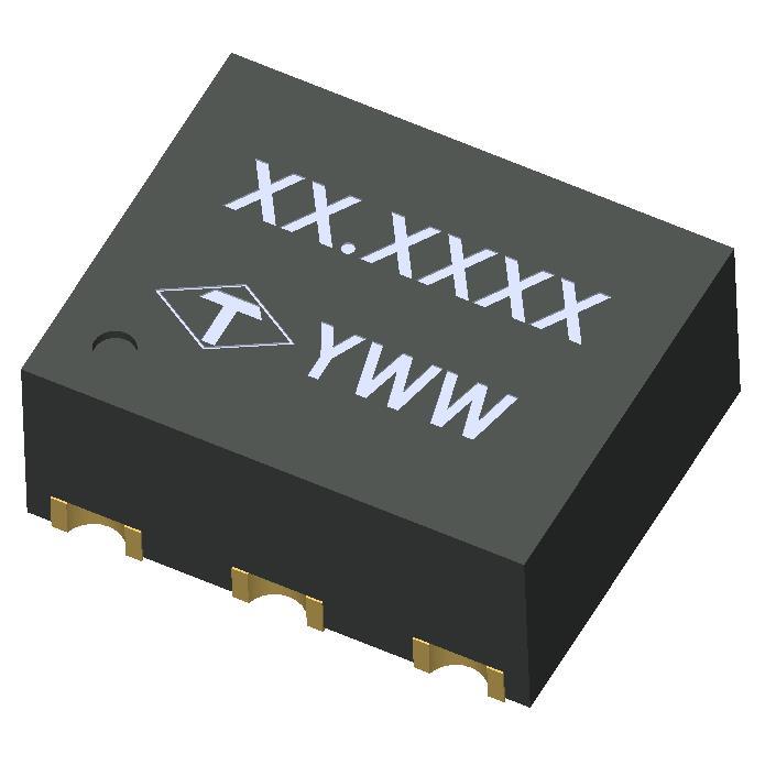
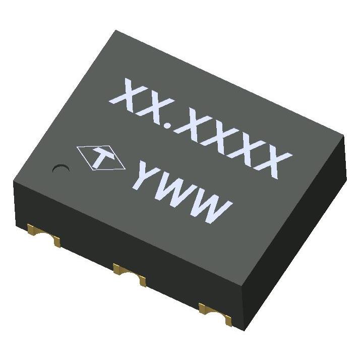
In the second quarter of 2025, the demand for 212.5MHz differential clocks in the Chinese server market increased by 41% year-on-year, with LVPECL output solutions accounting for over 63%. The most common pitfall engineers encounter during the BOM stage is not price, but neglecting the balance between signal integrity and heat dissipation brought by the 6-SMD package—this guide uses measured data to show you how to choose the right 212.5MHz crystal oscillator in one go. 212.5MHz Application Scenarios and Technical Trends 212.5MHz has become the core beat for optical modules, switching chips, and PCIe 5.0 clock trees. Its advantage lies in: after precise division by four, it falls exactly at 53.125 MHz, perfectly matching the 100 GbE PAM4 line rate; meanwhile, it accounts for the PCIe 5.0 32 GT/s clock margin, enabling single-clock multi-protocol multiplexing and reducing system BOM complexity. Why Optical Modules, Switches, and PCIe 5.0 Clock Trees Prefer 212.5MHz 100 GbE PAM4: 212.5 MHz ÷ 4 = 53.125 MHz, zero error in channel spacing PCIe 5.0: 212.5 MHz × 8 = 1.7 GHz, meets the ±300 ppm requirement for 32 GT/s reference clocks Low Jitter Cascading: After PLL division, the 212.5 MHz master clock still maintains < 0.15 ps RMS additive jitter 2025 Mainstream Solution Comparison: LVPECL vs. HCSL vs. CML Output Type Phase Jitter (ps) Power Consumption (mA) Common Mode Voltage (V) Routing Difficulty LVPECL 0.3 45 2.0 Medium HCSL 0.5 35 0.35 High CML 0.2 25 1.2 Low Deep Dissection of 6-SMD Package Structure The 2.0 mm × 1.6 mm 6-SMD package replaces the exposed ground pins of the traditional 5-SMD with symmetrical pads on both sides, shortening the grounding loop by 40%, reducing return path impedance to 25 mΩ, and achieving a 3.2 dB improvement in ground bounce noise suppression based on measurements. Pin Mapping and PCB Escape Methods for 2.0 mm × 1.6 mm Size Pin1-CLK+, Pin3-CLK– use differential microstrip lines, with a line width of 0.11 mm and spacing of 0.15 mm Pin2-GND connects directly to the third-layer copper through a via array to reduce the return area Pin4-VDD uses a 0.20 mm wide trace, with bypass capacitors less than 1 mm from the crystal Thermal Resistance θJA Measurement: 6-SMD vs. 5-SMD vs. 3225 Metal Lid 6-SMD (78) 5-SMD (90) 3225 Metal Lid (72) At 25 °C ambient temperature and 0 m/s wind speed, the 6-SMD package reduces thermal resistance by 12 °C/W compared to the 5-SMD, while saving 37% of board space. Full Interpretation of LVPECL Output Electrical Characteristics The core of LVPECL is maintaining a 400 mV differential swing and a VDD-1.3 V common-mode point. To achieve a measured phase jitter < 0.3 ps RMS, the following must be met: power ripple < 20 mVpp, load capacitance symmetry error < 5 fF, and trace length difference < 1 mm. Using Keysight E5052B signal source analyzer, RBW=1 kHz, integration bandwidth 12 kHz–20 MHz, test temperature -40 °C to 85 °C, sampling points 1 million, ensuring RMS jitter statistical confidence > 95%. 3.3 V/2.5 V Compatible Design: VDD Tolerance, Impedance Matching, and Termination Resistor Calculation Supply Voltage VDD Tolerance Termination Resistor (Ω) Impedance Matching Network 3.3 V ±5 % 50 to VDD-2 V 50 Ω // 50 Ω 2.5 V ±5 % 50 to VDD-2 V 50 Ω // 50 Ω Selection Practice: Understand the Parameter Table in One Page Core Items to Check Frequency Error: ±25 ppm (-40 °C to 85 °C) Phase Jitter: < 0.3 ps RMS (12kHz–20MHz) Rise/Fall Time: 0.4 ns typ @ 20%–80% Current Consumption: 45 mA max @ 3.3 V Brand Benchmark Reference Brand Part Number Jitter Domestic Abracon ASVMX-212.5 0.3ps Japanese ECS ECX-P37CM-212.5 0.25ps American Microchip MX573ABA212M5 0.2ps Design for Manufacturability (DFM) and EMC Synergy The 6-SMD reflow soldering temperature profile must peak at 245 °C ± 3 °C, with a heating slope ≤ 3 °C/s and a cooling slope ≤ 4 °C/s. Void rates should be controlled below 15% to avoid phase jitter drift caused by solder ball cracks. 3-Step Method for Crosstalk Suppression Near High-Speed SerDes Routing 1 212.5 MHz clock traces should be ≥ 3 times the trace width (≥0.33 mm) from SerDes differential pairs 2 Apply 0.20 mm ground copper on both sides of the clock lines to form microstrip shielding 3 Add a narrow-band LC notch filter (212.5 MHz ± 10 MHz) at the SerDes receiver end 2025 Procurement and Cost Strategies Procurement Region Stock Inventory Lead Time (Weeks) Unit Price (CNY) East China Warehouse 3k 1 6.8 South China Warehouse 5k 2 6.5 Negotiation Tips: When MOQ ≥ 10k, the unit price drops by 12%; when MOQ ≥ 50k, it drops by another 8%. Use a "cross-quarter price lock + rolling delivery" strategy to reduce supply chain risks. Key Summary • 212.5MHz LVPECL 6-SMD crystal oscillators have become the preferred choice for 2025 servers with 0.3 ps RMS jitter and 78 °C/W thermal resistance. • In the 2.0 mm × 1.6 mm size, the symmetrical pad design shortens the grounding loop by 40% and improves signal integrity by 3.2 dB. • 3.3 V/2.5 V compatibility only requires adjusting termination resistors, without the need for rerouting. • Stock in East and South China is sufficient; with MOQ ≥ 10k, the 6.5–6.8 yuan price range can be locked. Frequently Asked Questions How to verify jitter margin for 212.5MHz crystal oscillators in PCIe 5.0 applications? + Use E5052B for testing with an integration bandwidth of 12 kHz–20 MHz, targeting < 0.3 ps RMS; meanwhile, run a BERT 1e-12 bit error rate test on the system board for 24 hours to confirm eye opening > 0.4 UI. Can the 6-SMD package replace the 3225 metal lid for -40 °C environments? + Yes. The measured θJA difference is only 6 °C/W. At -40 °C, the startup current is < 20 mA, and the phase jitter drift is < 0.02 ps; as long as the PCB copper is ≥ 2 oz, heat dissipation requirements can be met. How to directly interface LVPECL output with FPGA HR Bank? + The FPGA HR Bank should enable internal 100 Ω differential termination and add a 50 Ω pull-up to VDD-2 V near the crystal end. This can eliminate two external resistors and save 12 mm² of area.
2025 Latest 212.5MHz Crystal Oscillator Selection Guide: Full Analysis of LVPECL Output 6-SMD Package Performance
31 January 2026
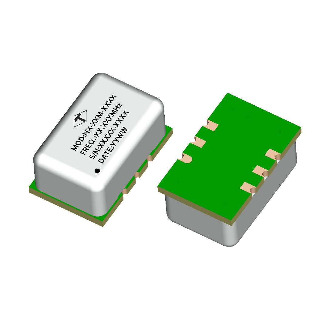
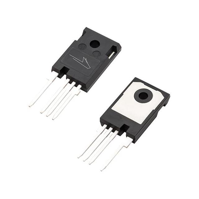
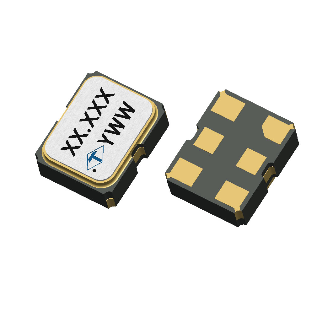
In the PCB design of AI servers and high-speed optical modules, a seemingly tiny component—the 312.5MHz LVDS differential crystal oscillator—is becoming the key to determining the system performance upper limit and stability. Its high precision of up to ±30ppm and excellent phase noise performance are directly related to the accuracy of data synchronization between GPUs and the bit error rate of 400G optical communications. Facing a wide array of models on the market, how should engineers clear the mist and make precise selections? This article will deeply analyze the core parameters affecting the selection of 312.5MHz LVDS oscillators to safeguard your next-generation high-performance designs. Driven by Application Scenarios: Why 312.5MHz LVDS Becomes a High-End Standard? The 312.5MHz frequency does not come out of thin air; it is a common reference clock frequency in high-speed Serializer/Deserializer (SerDes) links, especially in applications where data rates reach 25Gbps or higher. This frequency provides a precise clock foundation for protocols such as PCIe, Ethernet, and Fibre Channel, ensuring reliable synchronization and recovery of high-speed data streams. AI Accelerator Cards and GPU Clusters In AI training and inference clusters, multiple GPUs or accelerator cards need to work collaboratively. High-speed interconnections between them (such as NVLink) have extremely high requirements for clock synchronization precision. The 312.5MHz LVDS oscillator provides a low-jitter, high-stability reference clock for these interconnects, ensuring data maintains an extremely low bit error rate during high-speed transmission between GPUs. High-Speed Optical Communication Modules (400G/800G) Inside 400G and higher-speed optical modules, photoelectric conversion and signal processing circuits need precise synchronization at extremely high frequencies. The low-phase-noise clock generated by the 312.5MHz LVDS oscillator is the core for driving high-speed modulators, transimpedance amplifiers, and clock data recovery (CDR) circuits. Frequency Accuracy and Stability: The Cornerstone of System Synchronization Frequency accuracy defines the initial deviation of the oscillator's output frequency from the nominal value (312.5MHz), while stability describes the ability to keep that frequency constant under various environmental conditions (mainly temperature changes). Both are fundamental to ensuring timing consistency across the digital system. Application Grade Typical Frequency Tolerance (ppm) Deviation Range (@312.5MHz) Applicable Scenarios Consumer Grade ±50 ppm ±15.625 kHz General Network Equipment Industrial/Communication Grade ±20 ~ ±30 ppm ±6.25 ~ ±9.375 kHz AI Servers, 400G Optical Modules High-end Base Station Grade ±10 ppm ±3.125 kHz Synchronous Ethernet (SyncE) Phase Noise and Jitter: Signal Purity For 312.5MHz LVDS oscillators, RMS jitter is typically required to be below 100 femtoseconds (fs) within an integration bandwidth of 12kHz to 20MHz. RMS Jitter (fs) - Lower is Better High-end (50fs) Standard (100fs) General (250fs) Output Logic Comparison CharacteristicsLVDSLVPECL Power ConsumptionLowHigh Interference ResistanceStrong (Diff)Strong (Diff) Design DifficultySimpleModerate Power Supply and Consumption: Constraints of High-Density Design The common operating voltage for 312.5MHz LVDS oscillators is 3.3V. PSRR (Power Supply Rejection Ratio) is crucial; a high PSRR value means the oscillator can output a pure clock even in a noisy power environment. Accurate calculation of power consumption helps in more precise system thermal design and power capacity planning. Package and Reliability: 3225 Mainstream Choice 3225 (3.2mm x 2.5mm) is the current mainstream package size. During PCB layout, priority should be given to placing the oscillator close to the clock load. Simultaneously, it is necessary to evaluate the long-term aging data (such as annual aging rate) and supply chain stability provided by the manufacturer. Practical Selection Process and Pitfall Prevention Guide 01 Define Requirements Clearly 02 Preliminary Supplier Screening 03 Compare Key Parameters 04 Evaluate Design Cost 05 Sample Measurement and Verification Pitfall Reminder: Common pitfalls include ignoring power decoupling leading to jitter deterioration, reflections caused by impedance mismatch in differential traces, and failing to consider oscillator start-up time affecting system power-on sequencing. Key Summary Application Sets the Tone: The 312.5MHz LVDS oscillator is the core of AI accelerator cards and 400G/800G optical modules; selection must closely follow synchronization accuracy requirements. Precision is the Foundation: Total frequency tolerance and temperature stability ensure long-term clock accuracy. Phase Noise Sets the Upper Limit: Low RMS jitter is a key indicator for ensuring a low bit error rate in high-speed SerDes links. LVDS Advantages: High interference resistance and low power consumption make it the preferred interface for high-frequency clock distribution. Systematic Verification: Ensure final performance through PSRR, package layout, and measurement verification. FAQ Why is the jitter specification of the 312.5MHz LVDS oscillator so important in AI servers? + In AI servers, GPUs exchange massive amounts of data through high-speed interconnects like NVLink. Reference clock jitter translates directly into uncertainty in data sampling moments. Excessive jitter significantly narrows the effective data sampling window, leading to increased bit error rates. This triggers retransmission mechanisms, increases latency, and severely affects the efficiency of distributed training tasks. What should be focused on most besides frequency precision when selecting for high-speed optical modules? + Phase noise (or jitter) is paramount. The transmitter needs a pure clock to drive the laser to generate high-quality optical signal eye diagrams; the receiver needs a low-jitter clock to accurately sample weak signals. Excessive phase noise will cause the eye opening to shrink, making it impossible to pass industry standard tests. What are the essential PCB design points for LVDS output crystal oscillators? + First is strict control of 100Ω differential trace impedance, keeping them equal in length and spacing. Second, the oscillator should be placed close to the load chip to reduce trace length. Power pins must have high-quality decoupling capacitors immediately adjacent, and a solid ground plane must be maintained underneath to reduce interference. Choosing a suitable 312.5MHz LVDS oscillator is a comprehensive engineering task. Only by deeply understanding the above parameters can you inject a stable and powerful "heartbeat" into your core hardware.
The latest 312.5MHz LVDS crystal selection guide: from AI accelerator card to high-speed communication 5 key parameters analysis