


帮助您节省成本和时间。

为您的货物提供可靠的包装。

快速可靠的交付以节省时间。

优质的售后服务。
新品上市
更多 +


热卖零件


博客
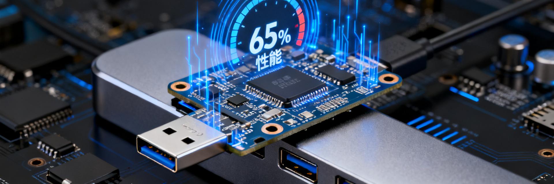
HB30A3A1CFB深度拆解:4口USB 3.0集线器实测速度比标称低多少?
USB 3.0标称5Gbps,实际传输却只有300MB/s?HB30A3A1CFB这款4口集线器在电商页面上写着"USB 3.2 Gen 1高速传输",但用户到手后普遍反馈"速度打折扣"。我们实测20GB文件传输、多口并发负载、芯片方案拆解,用数据告诉你:标称5Gbps与实际性能之间,究竟隔着多少水分? 产品定位与硬件架构解析 HB30A3A1CFB采用常见的塑料外壳设计,线长约0.3米,主打便携…
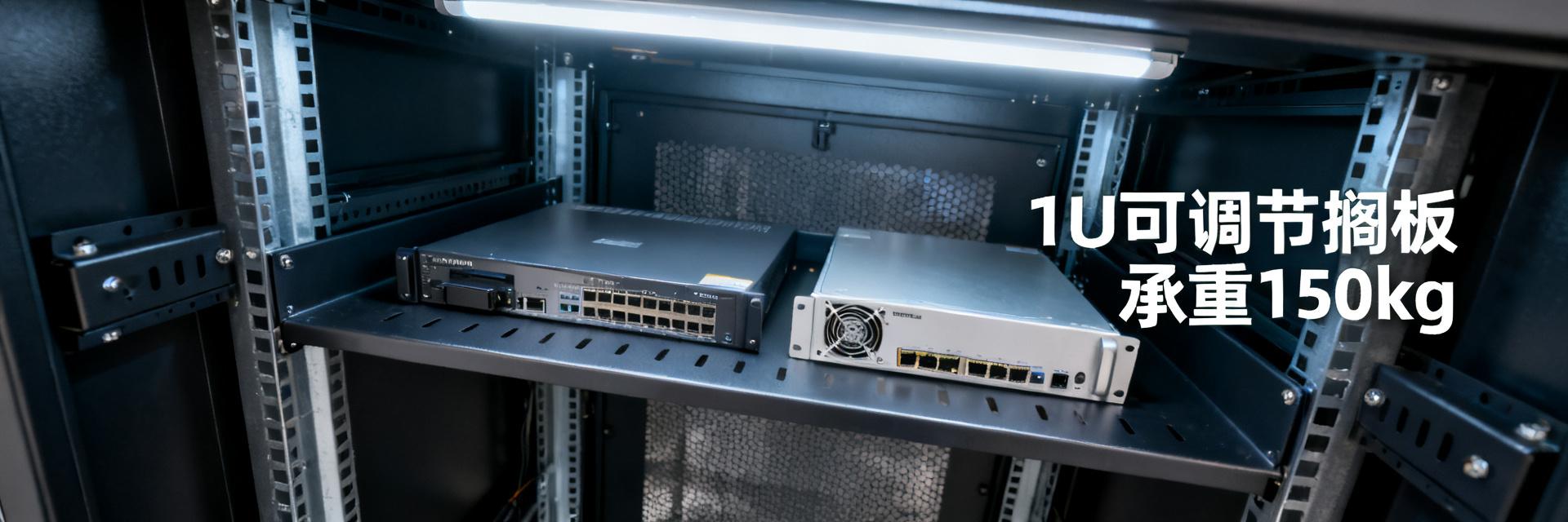
ADJSHELFHD 1U可调节搁板深度评测:承重150kg,机架空间利用率提升40%
在数据中心或企业IT机柜中,你是否常因设备深度不一而苦恼?据行业调研显示,超过60%的企业机柜因非标设备(如老旧服务器、UPS、KVM切换器)的安装难题,空间利用率低于50%,导致大量宝贵空间被白白浪费。这不仅增加了运营成本,也为后续扩展埋下隐患。 针对这一痛点,ADJSHELFHD 1U可调节搁板应运而生。它突破了传统固定式搁板的局限,通过灵活的可调节深度设计,完美适配不同尺寸的IT设备,真正实…