


帮助您节省成本和时间。

为您的货物提供可靠的包装。

快速可靠的交付以节省时间。

优质的售后服务。
新品上市
更多 +


热卖零件


博客
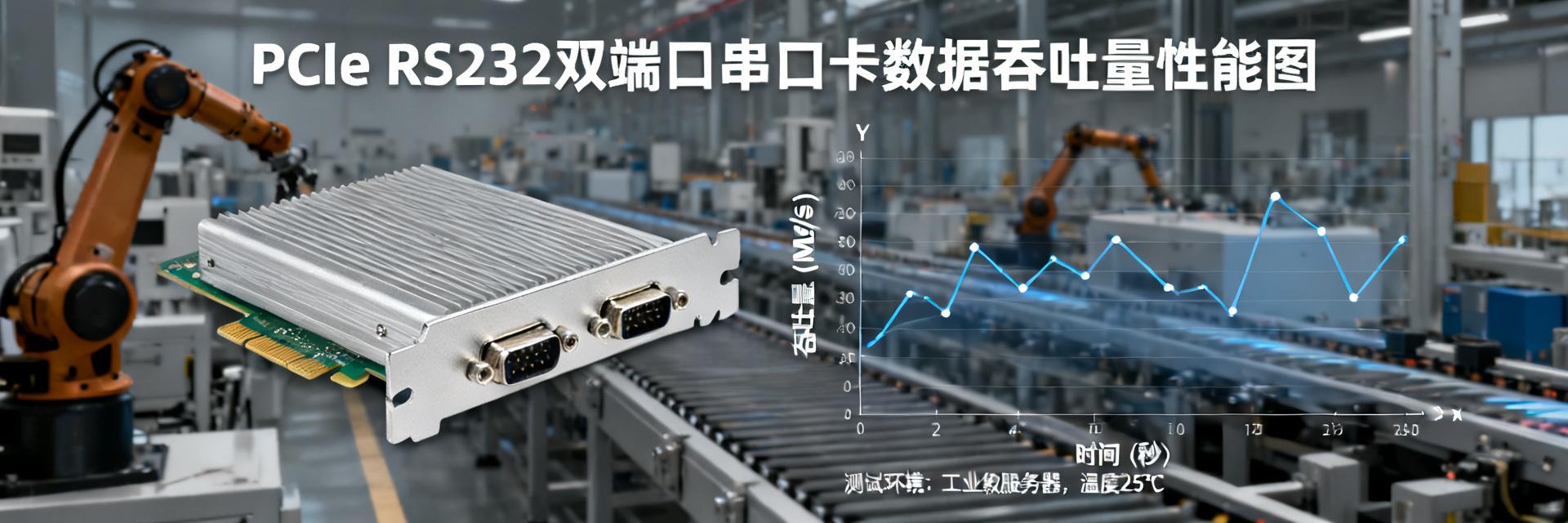
双端口PCIe RS232串口卡评测:数据吞吐量实测与性能对比
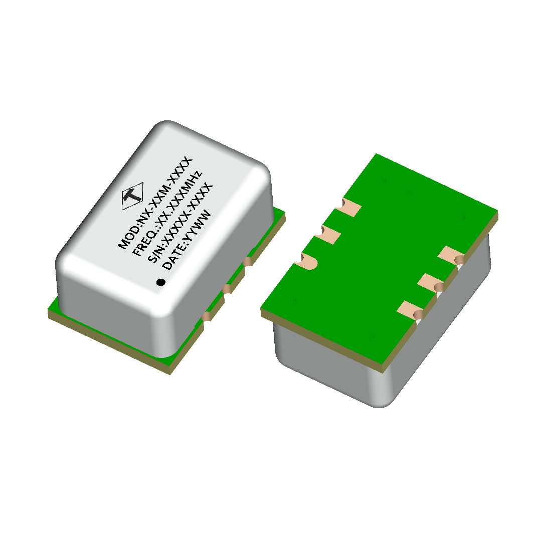
在工业自动化、金融终端和医疗设备等场景中,大量老旧但可靠的RS232串口设备依然是核心刚需。当现代主板逐步淘汰原生串口,PCIe串口卡便成了连接新旧世界的唯一桥梁。本文将通过实测数据,聚焦“数据吞吐量”与“传输稳定性”,揭示双端口PCIe串口卡的真实工业表现。 双端口PCIe RS232串口卡的市场背景与应用痛点 在数字化转型浪潮中,工控机、PLC、POS收银及实验室仪器仍大量依赖RS232协议。…
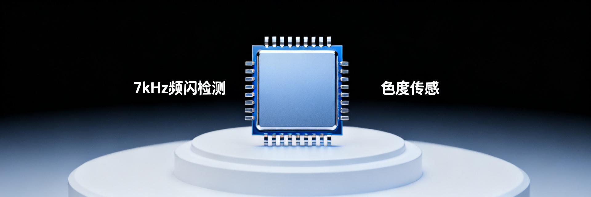
TCS35303-2技术解析:高精度真彩环境光与7kHz闪频检测突破
行业前沿 深度技术专题报告 在智能手机与显示器追求极致视觉体验的今天,自动白平衡(AWB)和屏下环境光感测的精度直接决定了用户的色彩感知。与此同时,源于PWM调光LED和OLED屏幕的频闪,正成为导致用户视觉疲劳的主要元凶。最新的TCS35303-2传感器,正以其独特的高精度真彩能力与业界领先的7kHz频闪检测范围,为这些痛点提供了全新的硬件级解决方案。 作为ams-OSRAM推出的新一代真彩传感…
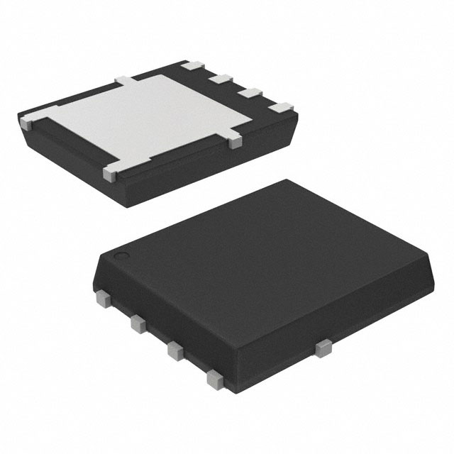
NVMYS4D5N04CTWG 数据手册精讲:40V N沟道 MOSFET 关键参数与特性全解析
2026-05-14 10:13:20
缺货危机?真实案例:某安防厂商如何用48小时搞定10K ASX340AT3C00XPED0-DPBR2
2026-05-07 10:25:17
2025国产60V MOSFET pin-to-pin替代清单:NVMFS5C604NWFT1G的5款高性价比数据报告
2026-05-03 10:13:17
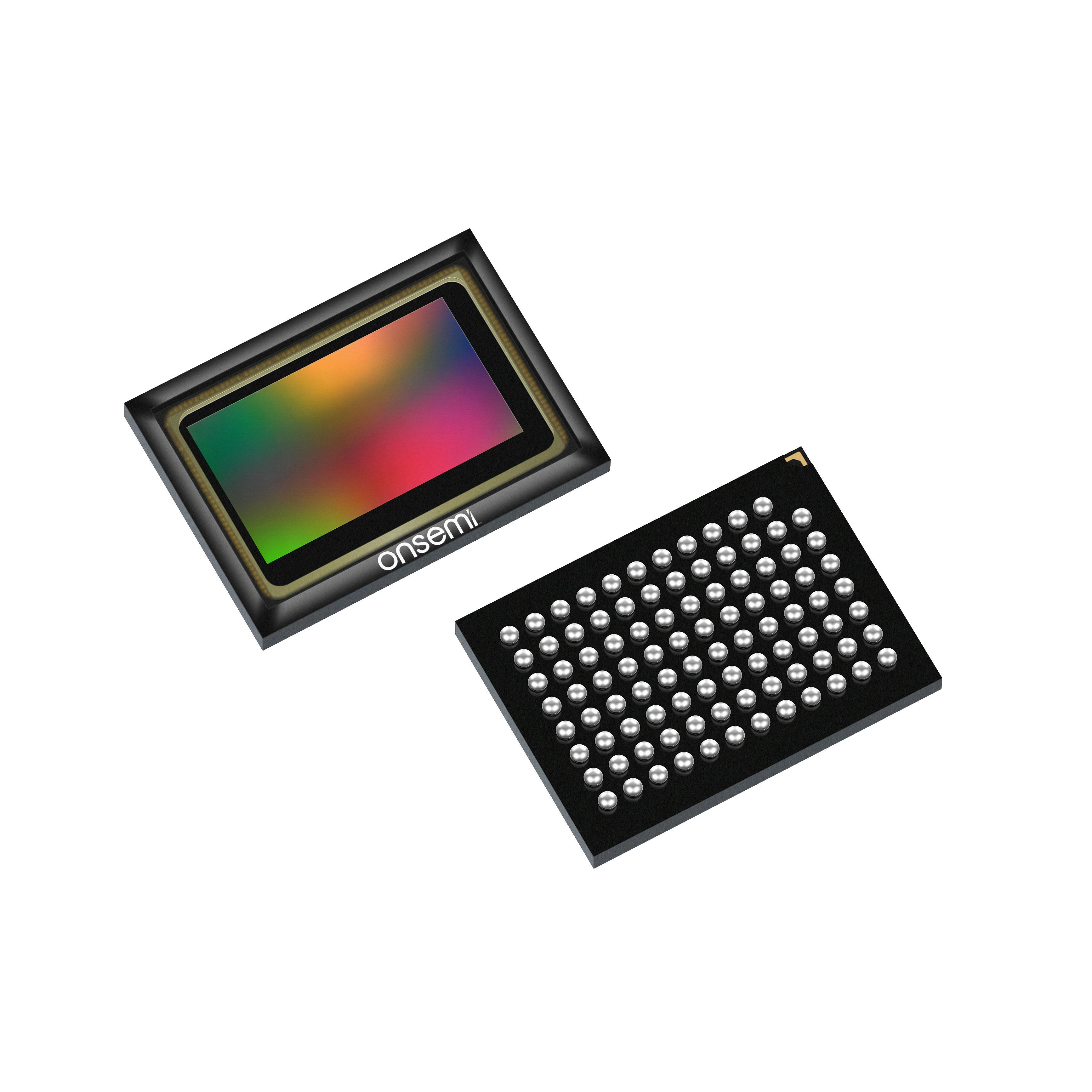
onsemi AR0830 选型终极指南:替代型号与性能对比
2026-05-01 10:14:21
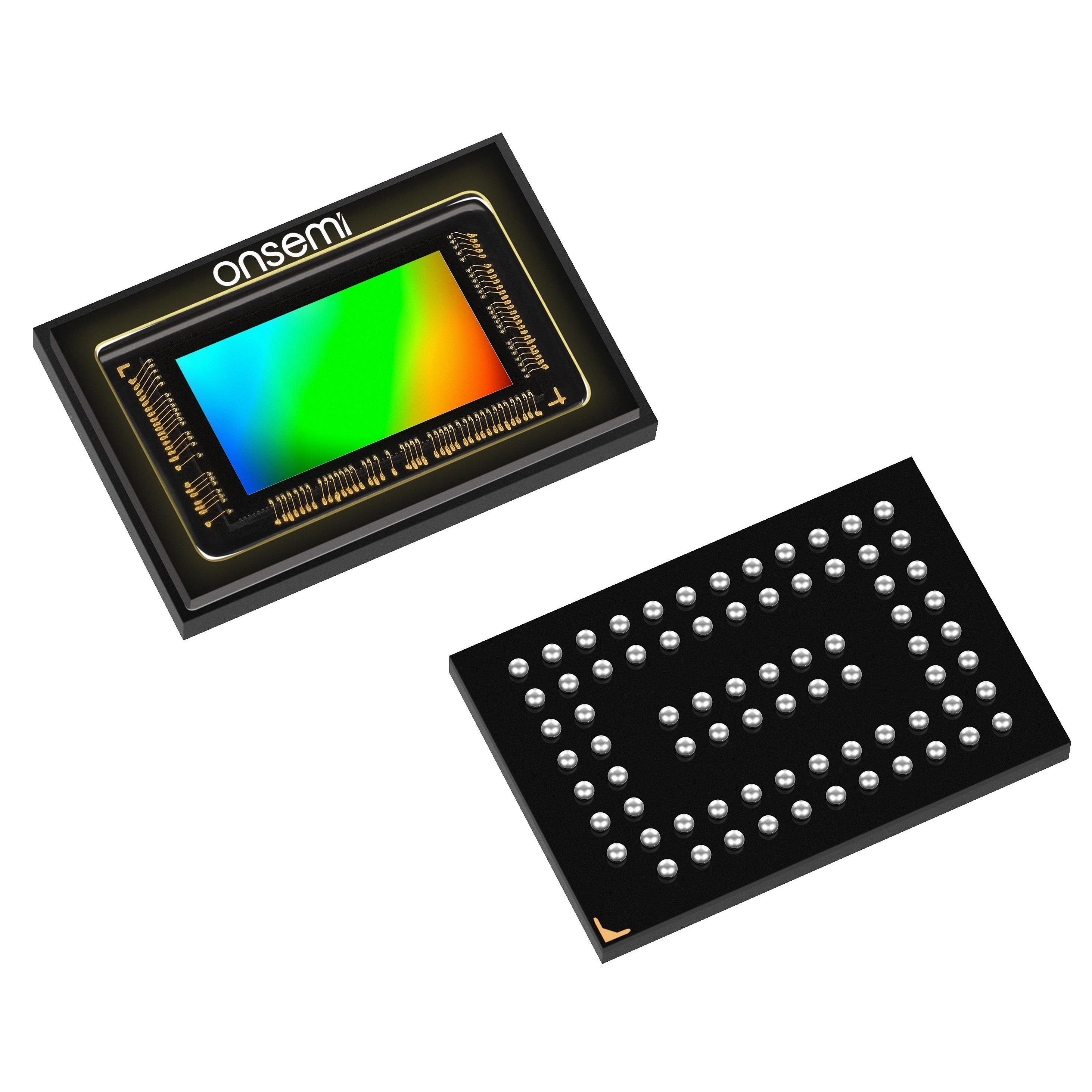
数据揭秘:20MP BSI CMOS传感器AR2020,为何成为机器视觉新宠?
2026-04-23 10:14:19
阅读更多